


Intel Foundry is moving forward with its 14A 1.4nm process node to support US chip independence and secure domestic technology leadership.
Intel is investing over $20 billion in Ohio to make AI and high-performance computing chips in the US using advanced EUV lithography.
Important Details And Impact
- The 14A node targets high-performance computing and AI and aligns with Intel’s plan to deploy five nodes over four years.
- Intel plans to build a site in Licking County for up to eight factories, aiming to begin production by 2030.
- By building advanced factories in the US, Intel will directly reduce reliance on foreign supply chains, strengthening US sovereignty over critical AI hardware.
- Intel uses EUV and Foveros Direct 3D stacking to improve packaging.
- Despite delays and the need for external customers, the 14A project remains central to US competitiveness in chipmaking and is supported by the CHIPS Act.
Intel’s 14A Node is a key product under development at Intel Foundry with a planned launch in 2027. As Intel collaborates with customers on the 14A design, clients can assess whether the new node meets their performance, efficiency, and market goals. Patrick Morehead from More Insights and Strategy, who regularly speaks with industry leaders, reports that two Intel customers are very satisfied with the progress of the node. Clients who have reviewed 14A note that it should deliver highly competitive capabilities for data center, PC, and mobile CHIPS—offering potential benefits such as enhanced performance, broader application scope, and early access to state-of-the-art technology.
He also said I am anxious for Intel to release its 14a 0.5 PDK and start gathering feedback. Even without the PDK available, I’m already hearing very positive things, especially considering the progress with 18a as each new node builds up on the previous ones.
Intel develops the 14A node using high-NA EUV to enable finer, more efficient chips. It leads the shift from low to high NA.
By reducing the number of steps per wafer layer from 40 to fewer than 10, Intel simplified manufacturing and sped up product delivery.
Customers emphasize security and adequate wafer allocation. Intel’s Twinscanexe:5200B processes 200 wafers per hour.
“Process Roadmap Expands Beyond 5N4Y”
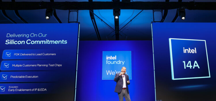
Intel has strengthened its Process Technology roadmap by adding Intel 14A to its leading-node plan, along with several specialized-node updates. The company confirmed that its five-node in four years (5N4Y) plan is still on schedule and will increase the industry’s first backside power solution. Leaders at Intel expect to regain process leadership with Intel 18A in 2025.
The updated roadmap includes improvements for Intel 3.0, 18A, and 14A process technologies. It also introduces Intel 3T, which uses through-silicon vias for 3D advanced packaging and will soon be ready for manufacturing. The roadmap also highlights mature process nodes, including the new 12nm nodes developed with UNC, as announced last month. These updates help customers create products that meet their needs. Intel Foundry plans to release a new node every two years, along with regular updates, so customers can keep improving their products using Intel’s latest technology.
Intel expanded its ASAT lineup, adding FCBGA2D+ to existing FCBGA 2D, AM, IB, Foveros, and Foveros Direct offerings.
Microsoft Design on Intel 18A Headlines Customer Momentum
Reflecting this exciting momentum, customers are enthusiastically backing Intel’s Long-Term Systems Foundry strategy. In Pat Gelsinger’s keynote, Microsoft Chairman and CEO Satya Nadella shared the exciting news that Intel has selected a chip design to manufacture using the Intel 18A process.
We are in the midst of a very exciting platform shift that will fundamentally transform productivity for every individual organization and the entire industry. Nadal has said: “To achieve this vision, we need a reliable supplier of the most advanced, high-performance, and high-quality semiconductors. That is why we are so excited to work with Intel Foundry and why we have chosen HF Design, which we plan to produce on Intel A-Process.”
With the exciting support of Microsoft, Intel Foundry has won designs across several process generations, including Intel 18A, Intel 16, and Intel III. The company is also experiencing strong customer enthusiasm for its ASAT capabilities, especially advanced packaging.
Bringing these successes together, Intel Foundry expects its lifetime deal value for wafers and advanced packaging to exceed $15 billion.
Source:
Intel 14A Node Trials Signal Confidence From Early Customers
Intel Launches World’s First Systems Foundry Designed for the AI Era