


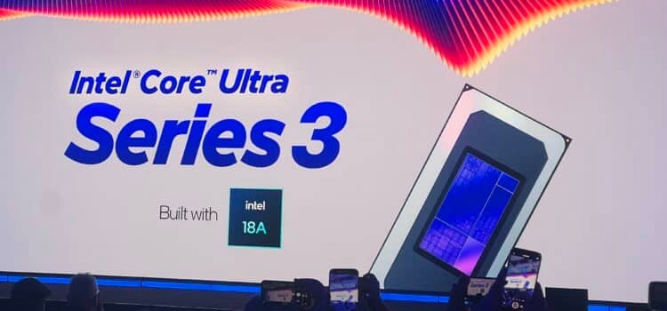
At CES 2026, Intel is launching its Intel Core Ultra Series 3 mobile chips based on the recently introduced Intel Panther Lake architecture. An advancement over the previous Core Ultra 200 series is the adoption of the new XE3 Graphic Cores, which offer improved performance and efficiency. Intel also revealed plans for a future handheld console platform built on Panther Lake, with more details to come this year.
Panther Lake brings additional non-graphics enhancements over prior generations and shifts to Intel’s 2NM18A process node for boosting performance and efficiency. Systems with Series 3 processors are already available.
The new chips use updated names. Series 3 indicates the generation, and NX means Intel Arc B390 graphics with maximum XE3 cores. Ultra 9 and Ultra 7 versions are available; Ultra 7’s GPU was benchmarked in November.
The Core Ultra 5 has Arc d370 graphics and no eX label. Only Arc Pro GPU performance data is available so far, and the 27-hour battery claim applies only to systems with this GPU.
Intel announced at its CES keynote that it will formally launch its first Core Ultra Series 3 laptop processors later this month. Code-named Panther Lake, these chips are initially aimed at high-end ultra-portable PCs. They will be the first to use the Intel 18A manufacturing process. This move is part of the company’s strategy to compete with Taiwan Semiconductor Manufacturing Company (TSMC).
The launch will begin with 14 chips across five product families, which Intel expects to appear in over 200 PC designs. The first chips will be available on January 27, with additional models released throughout the first half of the year.
The Core Ultra X9 and X7 processors feature Intel’s latest CPU and graphics processing unit designs. They include a fully enabled 12-core Intel Arc B390 iGPU and support faster LPDDR5X-9600 memory.
Core Ultra 9 and 7 processors also use Intel’s latest CPU and GPU technologies; however, these chips include only 4 GPU cores, while the X9 and X7 have 12 GB of GPU core memory. Additionally, the Ultra 9 and 7 offer 720 PCI Express lanes compared to the X9 and X7’s 12 lanes, making the Ultra 9 and 7 better suited for dedicated GPUs. Supported memory layer types for the Ultra 9 and 7 are either LPDDR5x-8533 or DDR5-72000 DIMMs. Unlike the faster LPDDR5x-9600 memory in the X9 and X7.
The Core Ultra 5 chips are mainly lower-end models with fewer CPU scores and either 4- or 2-core GPUs. However, the Core Ultra 5 338H stands out by featuring 12 CPU cores and a 10-core Intel Arc B370 GPU.
What Is Panther Lake?
Intel previously shared details about Panther Lake’s architecture late last year. In many respects, this chip Intel revealed at its CAS keynote shifts from the Lunar Lake design sold as Core Ultra 200V, which used externally manufactured chiplets and unpackaged RAM instead of DIMM slots or soldered memory. Intel stated that these adjustments are designed to save power and extend battery life, including the removal of hyper-threading support from the P-cores.
Core Ultra 3 chips reversed some of these changes, but Intel indicated it used Lunar Lake as a baseline for power efficiency to help ensure improvements do not compromise battery life.
As with previous Ultra Core Generations, the Core 3 Ultra Chips use a chip-like design. Several silicon tiles are combined on a base tile with Intel’s Faviros Packaging Technology.
- The compute tile built using 18A contains the CPU cores and Neural Processing Unit. It is available in versions with up to 16 or 18 CPU cores.
- The platform controller tile handles most I/O.
- The High-End 12-core graphics tile is produced at TSMC.
- A simpler four-core graphics tile uses the older Intel 3 process, which has mainly been used for Xeon server CPUs.
This chiplet-based strategy lets Intel offer three main Panther Lake configurations:
- 16-core CPU with a 12-core GPU
- 16-core CPU with a 4-core GPU
- Additional models with some CPU and GPU cores disabled
These complete the Core Ultra III series lineup.
Intel claims the top Core Ultra 3 processors deliver up to 60% faster multi-core CPU and up to 77% faster integrated GPU performance compared to Core Ultra 200 V chips. For instance, the Core Ultra X9388H on a Lenovo Ideapad reportedly streamed Netflix at 1080p for 27.1 hours though actual battery life depends on system choices.
All Panther Lake chips include the same Neural Processing Unit capable of up to 50 trillion operations per second. This exceeds the 40 TOPS required for Microsoft’s Co-Pilot Plus PC Label, though it is below the 60 TOPS claimed by AMD’s Ryzen AI 400 series and the 80 TOPS reported by Qualcomm’s Snapdragon X2 chips. Key connectivity features include Wi-Fi 7, Bluetooth 6, and up to four Thunderbolt 4 ports. It’s a key point for Intel’s fortunes or a temporary rebound in between years of missed deadlines. (Panther Lake is a month later than Intel said it would be in October, though by its recent standards, that isn’t bad.) However, their launch later this month suggests that the company’s AT&A facilities are up and running, opening the door to third-party chip manufacturing, a pursuit former CEO Pat Gelsinger began five years ago.
Intel 18A explained
Intel Foundry’s latest process technology introduces RibbonFET, the industry’s first Power Via backside power delivery, enabling customers to develop innovative designs.
Delivers up to 15% higher performance per watt and 30% greater chip density than the Intel 3 process node, enabling end-users to benefit from more powerful and efficient devices, and allowing manufacturers to produce more chips per wafer.
For the move, this is the first sub-2nm advanced node manufactured in North America, providing customers with a reliable supplier alternative.
PowerVia, the industry’s first backside delivery technology, increases density and cell utilization by 5 to 10% and reduces resistive power droop. This results in up to 4% improvement in ISO performance and significantly lowers the inherent resistance IR drop compared to frontside power designs.
The RibbonFET gate-all-around (GAA) transistor technology enables precise electrical current control. It supports further miniaturization of chip components and reduces power leakage, both of which are essential for high-density chips.
Omni-MIM capacitors significantly reduce inductive power droop, enhancing stable chip operation. This is essential for modern workloads such as Generative AI, which demand rapid, intense computational power.
Equally important are fully supported industry-standard EDA tools and reference flows. This technology enables a smooth transition from other nodes with EDA partners providing reference flows. Customers can begin designing with PowerVia before other backside power solutions become available.
Supported by over 35 leading ecosystem partners across EDA, IP, design services, cloud services, aerospace, and defense, this offering ensures broad customer enablement and simplifies adoption.


