


Critical Details
- Samsung has started mass production of HBM4, which offers a steady transfer speed of 11.7 Gbps and can reach up to 13 Gbps.
- The advanced DRAM uses a 4NM logic-based DAI to boost performance, reliability, and energy efficiency for future data centers.
- Samsung’s secure manufacturing process and strong supply chain support its HBM plans beyond HBM4.
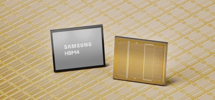
Samsung Electronics has announced it has started mass production of its HBM4 memory and has already shipped products to its customers. This makes Samsung the first company in the industry to reach this milestone and take an early lead in the HBM4 market.
By using its cutting-edge sixth-generation 10nm-class DRAM process, Samsung achieved stable yields and top performance from the start of mass production, without requiring additional redesigns.
Rather than using existing designs, Samsung chose to use the most advanced nodes, such as 1C DRAM and the 4nm logic process, for HBM4, said Sang Joon Hwang, Executive Vice President and Head of Memory Development at Samsung Electronics. By concentrating on process and design improvements, we can offer higher performance to meet our customers’ growing needs.
Raising the Standard Toward Performance and Efficiency
Samsung’s HBM4 runs at a steady 11.7 Gbps, about 46% faster than the industry standard of 8 Gbps and sets a new benchmark for HBM4. This is a 1.22 times increase over the previous HBM3E’s top speed of 9.6 Gbps. HBM4 can also reach up to 13 Gbps, helping to reduce data bottlenecks as AI models grow larger.
The total memory bandwidth per stack is now 2.7 times higher than HBM3e, reaching up to 3.3 terabytes per second (TB/s).
With 12-layer stacking, Samsung’s HBM4 comes in sizes from 24GB to 36GB. In the future, 16-layer stacking will allow for options up to 48GB, matching customer needs as they arise.
To handle higher power use and heat from doubling data I/O from 1024 to 2048 pins, Samsung has added advanced low-power designs to the core die. HBM4 is 40% more power efficient thanks to low-voltage TSV technology and PDN optimization. It also improves thermal resistance by 10% and heat dissipation by 30% compared to HBM3e.
With its excellence, performance, energy efficiency, and reliability, Samsung’s HBM4 helps customers get the most from their GPUs and better control their total cost of ownership.
Comprehensive Yet Agile Production Facilities
Samsung is moving its HBM roadmap forward by using its broad manufacturing resources, which include one of the largest DRAM production capacities and dedicated industry infrastructure. This solution helps keep the supply chain strong and ready for the unexpected rise in HBM4 demand.
By closely coordinating its foundry and memory businesses through design technology and co-optimization (DTCO), Samsung maintains high quality and strong yields. Its in-house skills in advanced packaging also help speed up production and shorten lead times.
Samsung plans to expand its technical partnerships, working closely with global GPU makers and hyperscalers, to develop next-generation ASICs.
Samsung expects its HBM sales to more than triple in 2026 compared to 2025 and is already increasing its HBM4 production capacity. After HBM4 launches, HBM4E samples should be available in the second half of 2021, and custom HBM samples will be delivered to customers in 2027 as needed.
Source: Samsung Ships Industry-First Commercial HBM4 With Ultimate Performance for AI Computing


