


With AI semiconductors set to be a key topic at the upcoming South Korea-U.S. summit on August 25th, major domestic semiconductor companies, including Samsung Electronics and SK Hynix, are finalizing additional U.S. investment plans. The Samsung U.S. chip plant is considering expanding its local investments, including a 10 trillion won investment in packaging facilities previously excluded from last year’s plan, after securing significant 6 orders from U.S. tech companies, Tesla, and Apple.
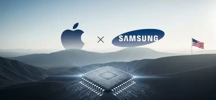
According to industry sources on August 11, Samsung Electronics had initially planned a $44 billion investment in its Samsung Foundry plant in Taylor, Texas, but reduced it to $37 billion at the end of last year due to poor performance. The original plan included four NM and two NM Foundry plants, as well as advanced packaging and R&D facilities, but the $7 billion advanced packaging investment was omitted due to difficulties securing customers.
Following a 2.3 trillion won AI semiconductor supply contract with Tesla on July 28 and an Apple image sensor order soon after, Samsung Electronics now sees an increased need for an advanced packaging plant. To avoid US tariff pressure, the full process from chip manufacturing in the US to post-processing must occur locally. Samsung’s key advantage in securing major tech clients is in its turnkey service, which integrates memory, foundry, and packaging.
Investment is expected to rise not only in packaging but also in equipment and materials. By the end of the first quarter, construction of Taylor Fab One was 91.8% complete, with overall completion planned for October. The clean room is scheduled for completion by year-end, with semiconductor production equipment to be installed next year. A high-ranking official from a materials supplier to the Taylor plant stated, “I understand that discussions are in progress to expand supply volumes in preparation for increased local investment.”
Tesla’s orders may exceed the initially announced scale, potentially triggering additional investment in equipment and materials. Elon Musk, CEO of Tesla, previously stated regarding the contract with Samsung’s Foundry, “The figure of $65.5 billion is just the minimum amount, adding the actual production volume is likely to be several times more.” This indicates the Tesla order could expand beyond vehicle chips to include Samsung semiconductors in the US for supercomputers and other electronic equipment.
Samsung Electronics also stated during its performance announcement last month that this year’s investment in the Taylor Fab will proceed within the existing capex (capital expenditure) plan, but we expect an increase next year. A senior industry official added, “Including additional investment in the packaging plant (Samsung’s investment in the Taylor plant will exceed $50B in West Lafayette, Indiana, for the production of high bandwidth memory (HBM) and other products, it is now on the verge of breaking ground.” The plan is to mass-produce next-generation HBM and other products from the second half of 2028. There is a possibility of expanding the investment scale by advancing the proper operational timing or increasing the number of production items beyond packaging.
The expansion of U.S. semiconductor investments by Samsung Electronics and SK Hynix is expected to support the upcoming South Korea-U.S. summit in Washington, D.C. Yoon Sung-hyuk, industrial policy secretary at the Office of the President, stated: “The existing investment plans for our companies in the U.S. will be included in the investment amount at the time of the summit.” Adding: “There are plans announced during the Joe Biden administration, like Samsung’s Taylor fab, but these plans will now proceed with chip orders from Tesla and will mainly be executed during the Donald Trump administration, effectively announcing an investment expansion” to indicate the strategic reasons behind the decision.
Regarding the latest updates about the New Plant Announcement and innovations in semiconductor plant construction, attend the second Construction Semiconductor FAB Summit Europe: Advances in Planning, Design, and Engineering on October 21-22, 2025, in Munich, Germany. The event will feature solution providers and expert speakers.


