


Mass production of HBM4 commences with a consistent transfer speed of 11.7 Gbps with a maximum of 13 Gbps.
Leading Edge DRAM with a 4nm logic-based die maximizes performance, reliability, and energy efficiency for next-gen data centers.
Secure Process Technology and Supply Capabilities Strengthen Samsung’s HBM Roadmap Beyond HBM4.
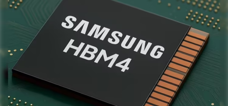
Samsung Electronics announced it has started mass production of its HBM4 memory and has shipped products to its customers. This makes Samsung the first company in the industry to reach this milestone and take an early lead in the HBM4 market.
By using its cutting-edge 6th-generation 10-nanometer (NM)-class DRAM Process (1C), Samsung achieved stable yields and top performance from the start of mass production without needing any extra redesigns.
Instead of using proven designs, Samsung chose the most advanced nodes, such as 1C DRAM and a 4nm logic process, for HBM4, said Sang Joon Hwang, Executive Vice President and Head of Memory Development. By leveraging our process strengths and design optimization, we deliver greater performance and can meet customers’ growing needs for higher performance when they need it.
Setting the Bar for Maximum Effectiveness and Efficiency
Samsung’s HBM4 operates at a data rate of 11.7 Gbps, which is approximately 46% faster than the prevailing industry standard of 8 Gbps. This represents a 22% increase over HBM3E’s maximum data rate of 9.6 Gbps. HBM4 can achieve peak speeds of up to 13 Gbps, alleviating bandwidth constraints as AI model sizes increase.
The aggregate bandwidth per HBM4 stack is now 2.7 times the weight of HBM3E, reaching up to 3.3 terabytes per second (TB/s) across all I/O pins. Samsung’s HBM4 uses a 12-layer 3D stacking approach with capacities ranging from 24 GB to 36 GB per stack. Future 16-layer stacks will support modules up to 48 GB, enabling scalability based on system and customer requirements.
To support increased power and heat from doubling data I/O from 1024 to 2048 signal pins, Samsung integrated advanced low-power circuitry at the core die. HBM4 achieves 40% higher power efficiency through low voltage, through-silicon vias (TSVs), and power distribution network (PDN) tuning, and realizes a 10% gain in thermal resistance and 30% better heat dissipation versus HBM3E. Samsung’s HBM4 delivers high performance, efficiency, and reliability, helping customers get more from their GPUs and control costs in new data centers.
Comprehensive Yet Agile Manufacturing Capacities
Samsung will build on its large-scale manufacturing resources to advance HBM4 and future technologies. The company will roll out enhancements and revisions to the roadmap in upcoming product generations.
Close collaboration between Samsung’s factory and memory teams through design-technology co-optimization (DTCO) supports maintaining high quality and yield. Their in-house expertise in advanced packaging also shortens production cycles and lead times.
Samsung also plans to expand its technical partnerships. The company works closely with global GPU makers and hyperscalers on next-generation ASIC development.
Samsung expects its HBM sales to more than triple in 2026 compared to 2025. The company is expanding HBM4 production with HBM4E sampling to begin in the second half of 2026, following the HBM4 launch. Custom HBM samples will be delivered to customers in 2027 as needed, outlining a sequential roadmap: first launch, then sampling, then HBM delivery.
Source: Samsung Ships Industry-First Commercial HBM4 With Ultimate Performance for AI Computing


