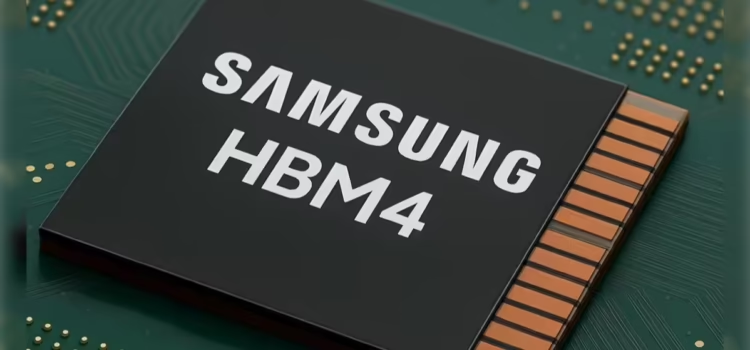


Samsung Electronics unveiled its 7th-generation high-bandwidth HBM4E at NVIDIA GTX 2026 in San Jose on Monday and plans to ship samples by mid-2026.
This marks Samsung’s first demonstration of its next-generation memory technology before mass production, strengthening its position as a supplier of advanced memory AI systems.
According to Samsung, its HBM4E chips each support a read data rate of 16 Gbps per pin. This is 36% faster than the previous generation’s 11 Gbps and twice as fast as the current industry standard of 8 Gbps. The chips also offer 4 TB/s of bandwidth, the maximum rate at which the memory can transfer data.
Samsung expects to deliver samples of the standard HBM4E products to customers in mid-2026. Custom versions of the chips, designed for specific processors and called application-specific integrated circuits (ASIC) solutions, are set to begin initial VFAP production on several projects in the second half of the year.
Samsung also confirmed that its 6th-generation HBM4 memory, which is distinct from the neural-oriented HBM4E, will be used in Vera Rubin and Media’s AI computing platform. Mass production of HBM4 (not HBM4E) began in February.
The HBM4 uses advanced DRAM and logic processes for memory control.
The sixth-generation chips reach 11.7 Gbps and may be further optimized.
Samsung demonstrated hybrid copper bonding, a new packaging technology that improves die-to-die connectivity and heat dissipation methods compared to current methods.
Samsung’s booth featured a special media gallery to highlight its supplier partnership. In addition to HBM4, Samsung displayed several products for AI infrastructure, including SoCAMM2, non-power-server DRAM modules, and the PM1763 solid‑state drive.
The company also introduced LPDDR5X and LPDDR6 mobile memory for AI workloads on personal devices. LPDDR5X reaches speeds up to 25 GB/s and reduces power use by up to 15%. LPDDR6 increases memory bandwidth to 30–35 Gbps.
For a hands-on experience and to learn more about Samsung’s innovative AI solutions, we invite you to visit booth 1207 at GTC 2026.
The highlight of Samsung’s display at NVIDIA GTC 2026 is the new 6th-generation HBM4, now in mass production and made for NVIDIA. Variable-bin platform. HBM4 is set to speed up future AI applications, offering steady data rates of 11.6 gigabits per second (Gbps) above the industry standard of 8 Gbps, and can be boosted to 13 Gbps.
Samsung’s advanced 10nm-class DRAM process powers HBM4 and the next-generation HBM4E, delivering top-tier quality and performance. Both products will be on display at GTC 2026.
Samsung will showcase hybrid copper bonding technology, which enables next-generation HPM to scale to more layers and lowers heat resistance.
An Alliance Taking the AI Era to a New Level
Samsung and NVIDIA’s close partnership will be featured in a special NVIDIA gallery at the booth. The gallery showcases a wide range of Samsung’s latest technologies, including HBM4, SoCAMM2, and the PM1763 SSD, in our design for in-air infrastructure.
Samsung’s SoCAMM2, now in mass production, is the industry’s first low-power DRAM server memory model, delivering efficient, scalable AI system performance with high bandwidth and flexible integration for next-gen infrastructure.
The PM1763 SSD leverages PCIe 6.0 for fast data transfers and capacity demonstrated on servers using NVIDIA’s programming model.
Samsung’s PM1763 SSD is part of the new NVIDIA BlueField-4 STX Reference Architecture, a blueprint for building AI-optimized storage systems to deliver faster storage on the NVIDIA Vera Rubin platform. It will demonstrate how it improves energy efficiency and system performance for inference workloads tasks where AI systems generate outputs based on data.
Memory Architecture To Scale, Intelligent Manufacturing
At GTC 2026, Samsung will showcase its work with NVIDIA on developing an AI factory and an automated, AI-assisted chip manufacturing system. This includes plans to use NVIDIA-accelerated computing and specialized processing for AI tasks to expand Samsung’s AI factory and speed up digital-twin manufacturing, where digital copies of factories are used for simulation with NVIDIA libraries and tools for virtual collaboration. Together, they support one of the world’s most complete chip manufacturing systems covering memory, logic, foundry, and advanced packaging.
Yong Ho Song, Executive Vice President at Samsung Electronics, will discuss the company’s strategic partnership and its AI and digital twin initiatives in transforming semiconductor manufacturing in his GTC 2026 talk.
Effective Memory For Local Intelligence
Samsung’s memory solutions also enable high-efficiency local AI on personal devices. At GTC 2026, Samsung will present customized and efficient options for personal AI supercomputers, including the PM9E3 and PM9E1. NAND types of flash memory for Nvidia DJX Spark
Samsung will also showcase DRAM (Dynamic Random Access Memory) Solutions, including LPDDR5X and LPDDR6, low-power DDR (double data rate) memory designed for easy use in smartphones, tablets, and other devices. These offer faster data speeds and lower latency. LPDDR5X reaches up to 25 Gbps and reduces power use by up to 15%, enabling fast mobile experiences, high-resolution gaming, and AI features without draining the battery.
Building on this, LPDDR6 increases bandwidth to a scalable 32–35 Gbps per pin and adds advanced power-management features, including productive voltage scaling and dynamic refresh control. These features deliver the performance required for upcoming edge AI workloads.
Source:
Samsung unveils HBM4E at Nvidia GTC, raises bar for AI memory