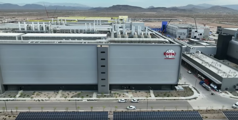


By December 23, 2025, global semiconductor manufacturing is at a major turning point. Taiwan Semiconductor Manufacturing Company (NYSE: TSMC), the world’s top contract chipmaker, has sped up its plans for the large Fab21 complex in Phoenix, Arizona. Phase one is already producing large volumes of 4 nm and 5 nm chips, and the company has started installing equipment and preparing clean rooms for phase two, which will make 3 nm chips. This progress is a big win for the US effort to bring key technology back home and strengthen the supply chain for future artificial intelligence.
The acceleration at the Arizona site, which previously faced labor issues and construction delays, marks a turning point for the American “Silicon Desert”. It not only demonstrates renewed confidence but also sets the stage for the next technical leap by moving up the 3nm production timeline to 2027, a year earlier than expected. TSMC is meeting strong demand from US tech companies seeking to protect their AI hardware from risks in the Pacific region.
Technical Milestones and the 92% Yield Breakthrough
Fab 21’s achievements have silenced early doubters about US advanced manufacturing. TSMC reported that its Arizona Phase 1 facility achieved a 92% yield rate in 4nm production, about 4 points higher than similar sites in Taiwan. This success stems from digital twin technology enabling virtual process optimization before real-world implementations.
Phase two’s shift to 3 NM technology advances both transistor density and energy efficiency. The 3 NM process offers up to 15% higher speeds at the same power or 30% lower power at the same speed compared to 5 NM chips. By December 2025, phase two’s building was complete, and interior installation for clean rooms and equipment was progressing rapidly. EUV lithography machines are set to arrive in early 2026 for 2027 production.
A Windfall for AI Giants End-to-End Supply Chain
Accelerated 3 nm output in Arizona benefits large AI companies. Apple, Nvidia, and AMD have reserved most of Fab 21’s capacity. For Nvidia, domestic production reduces shipping risks associated with the Taiwan Strait. Amkor Technology is constructing a $7 billion advanced packaging facility in Peoria, Arizona, contributing to the supply chain.
TSMC and Amkor’s partnership will enable the US supply chain to produce AI chips from fabrication through advanced packaging. Previously, US-made chips still needed to be shipped to Taiwan for packaging, creating risks. With local packaging, firms like Nvidia and AMD can achieve faster, more secure North American supply chains for AI.
The Geopolitical Significance of the Silicon Desert
TSMC’s Arizona expansion is extremely important. It is the highlight of the US Chips and Science Act, which gave TSMC 6.6 billion dollars in grants and up to 5 billion dollars in loans. By late 2025, the US Department of Commerce had released several rounds of this funding, noting TSMC’s strong technical progress. This puts the US in a better position against global competitors such as Samsung (KRX:005930) and Intel (Nasdaq:INTC), which are also working to launch advanced chip technologies.
This shift toward geographic decoupling is a direct answer to rising tensions in the South China Sea. By building a gigafab cluster in Arizona, expected to include six fabs and $165 billion in investment, TSMC is creating a secure backup to its Taiwan operations. This move has changed the global semiconductor industry, bringing high-end manufacturing closer to Silicon Valley’s software and design centers.
Looking Ahead: The Road to 2nm and Beyond
TSMC’s Arizona ambitions extend well into the future,d beyond current achievements. In April 2025, construction began on phase three,which will eventually produce advanced 2 nm and 1.6 nm chips needed for the next generation of AI models requiring greater power and efficiency. According to projections, by 2030, Arizona could match the capabilities of TSMC’s Fab 18 in Tainan, delivering the world’s most advanced chips.
Challenges remain, mainly a shortage of specialized talent to run automated fabs. The 92% yield shows early staffing problems are mostly solved, but expansion from two to six fabs over five years will require more engineers and technicians. Adding advanced packaging on-site will require TSMC and partners to work closely together. Accelerated 3nm equipment installation and high yields have turned the Silicon Desert from ambition to reality. This is a vital safeguard for US AI and national security.
As the next phase takes shape, anticipation continues to grow. In 2026, attention will focus on the arrival of EUV tools for phase two and progress on phase three. Supported by the Chips Act and major technology partners, TSMC Arizona sets a benchmark for domestic advanced chip manufacturing.
Source: TSMC Arizona’s 3nm Acceleration: Bringing Advanced Manufacturing to US Soil


