






Santa Clara, California
The era of the semiconductor industry, in which merely miniaturizing computer chips would ensure further advancements in computing, is over. Chip companies relied on scaling transistors down for decades as an essential tool to improve computing capacity. But now, the limitations of the process of miniaturizing transistors in silicon production are becoming increasingly evident.
Intel now believes the future of AI hardware will not rely on shrinking chips but rather on how multiple chips work together in a single semiconductor package.
It is one of the foundations of Intel EMIB Packaging technology, which the company announced in the latest engineering update presented today. According to Intel engineers, advanced packaging systems will be a key factor in their pursuit of dominance in AI infrastructure.
In turn, the expansion of the amount and complexity of data processed by AI leads to an increasing demand for higher Memory Bandwidth, greater efficiency, and greater scalability of computer processes.
Intel claims that multi-chip packaging technology may now be the future of semiconductor design.
What is Intel EMIB Packaging?
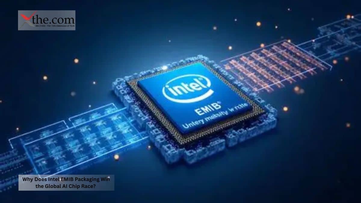
Intel EMIB Packaging means Embedded Multi-Die Bridge. Instead of making a single large silicon die, Intel uses multiple tiny dies that are joined into a single package via a high-speed, highly efficient communication bridge.
These small bridges act as super-fast interconnects, enabling separate processing dies to communicate as if they were one huge processor.
According to Intel engineers, the new packaging technology offers several significant benefits over monolithic chip manufacturing.
Since workload is split across smaller, interconnected dies, Intel can ensure greater manufacturing flexibility, along with lower production complexity and costs.
Moreover, Silicon Interconnect efficiency will be enhanced with the formation of fast communication paths between different memory systems, AI accelerators, and processing engines.
According to Intel engineers, this technology enables:
- Faster inter-die communication
- Better thermal balance
- Increased scalability of processing
- Less production waste
- Increased production flexibility
- Decreased workload latency
These benefits are essential in today’s complex AI infrastructure.
Why Good Packaging Is Important for Artificial Intelligence Infrastructure
There are many data movements between processors and memory systems to handle artificial intelligence tasks. Sometimes the chip design cannot deliver enough bandwidth without causing traffic jams.
Memory Bandwidth becomes an important element in this case.
AI systems operate on vast databases and need to perform millions, or even trillions, of computations simultaneously. This places heavy strain on memory and interconnect systems in data centers.
According to Intel, EMIB enables efficient data transfer between processing chips while minimizing their energy consumption.
Also, Intel pointed out that artificial intelligence infrastructure no longer relies solely on processor performance but also considers system architecture.
Intel hopes that improving its silicon interconnect performance will give it a competitive advantage over NVIDIA, AMD, and TSMC.
Embedded Multi-Die Bridge Technology Process
The Embedded Multi-Die Bridge Technology operates by installing tiny silicon bridges in the processor package substrate.
This connection of chiplets via extremely fast communication channels enables faster data exchange between processing elements.
Typically, other packaging technologies use longer communication channels, which introduce additional latency and heat.
According to Intel, its Embedded Multi-Die Bridge Technology is responsible for enhancing:
- AI training efficiency
- Inference processing capability at scale
- Data transfer efficiency
- Reliability
- Scalability for high-performance computing
This innovative packaging also facilitates better utilization of Intel’s specialized chip components.
Instead of developing a single large-scale processor to meet every requirement, Intel can assemble custom processing solutions tailored to specific enterprise workloads.
The recently discussed Intel EMIB advanced packaging hardware architecture specs further highlight Intel’s strategy for scalable AI infrastructure deployment.
The Significance of Kilowatt Power Consumption
The most pressing problem AI infrastructure providers face today is rising energy consumption.
Contemporary AI centers consume large amounts of power, particularly during the massive training of models. Today, certain enterprise AI services are beginning to demand infrastructure that spans Kilowatt Power levels, unlike any other computing system.
This trend poses many problems to both cloud and enterprise clients.
According to Intel, new packaging technologies may help address energy losses by reducing communication lengths and improving workload balance efficiency.
Better-designed package solutions would help reduce power waste and manage heat dissipation more efficiently. To succeed in the AI market, Intel believes that, in the future, the competitiveness of such systems will be based on balancing processing power with energy consumption. The rollout of Intel’s new packaging technology is significant for many other reasons, geopolitically speaking.
At present, the USA is striving to develop domestic semiconductor manufacturing capabilities and reduce its reliance on chip imports from China. Advanced chip packaging methods can ensure the competitiveness of US businesses despite limitations in transistor shrinkage. According to analysts, modular chip assembly could become one of the key semiconductor innovations in the next ten years.
In addition, EMIB-based technology may be cheaper for enterprise processors due to improved manufacturing yields with smaller chips. Intel’s plans for an AI Chip Foundry business will be highly contingent on leadership in advanced packaging technologies suitable for AI-specific needs.
Enterprise AI Infrastructure Rivalry
AI infrastructure competition has intensified dramatically as more money gets invested in enterprise-scale computing power.
Modern corporations cannot rely solely on processor speed; they should also focus on packaging, cooling systems, and memory architecture.
Intel expects to gain a competitive advantage by processing data across multiple cores using its unique EMIB technology.
Finally, the introduction of EMIB packaging technology specs may affect future chip design strategies in the semiconductor industry.
More analysts are forecasting an increase in the use of modular multi-die technology across companies due to the rapid scaling of AI workloads.
Conclusion
The new advancements in Intel EMIB Packaging represent one of the key turning points in the semiconductor industry towards the development of AI hardware.
Unlike traditional methods for improving performance by using smaller transistors, the new method emphasizes advanced packaging that enables multiple processing dies to function together within a single architecture.
Through increased Memory Bandwidth, lower latency, and improvements to Silicon Interconnect, Intel aims to establish itself as the leading infrastructure supplier for the next generation of AI computing.
Given the current trends, Intel EMIB Packaging is bound to play a crucial role in semiconductor innovation.
Source- Intel Newsroom