


As AI competition intensifies, many saw silicon’s physical limits as insurmountable. Taiwan Semiconductor Manufacturing Company, TSMC, has advanced these limits with the A16 process node: a 1.6 nm charge technology targeting mass production in the second half of 2026. This shift in chip design addresses not only further transistor miniaturization but also innovations in power delivery and thermal management.
The A16 node stands out for breaking from traditional manufacturing methods. With its new Super Power Retail (SPR) technology, TSMC is tackling the power wall that has slowed the development of next-gen AI chips. By the end of 2025, major AI companies will have already shifted their hardware plans to match this 1.6 nm milestone. A16 is more than a minor upgrade; it will serve as the foundation for the next decade of generative AI and high-performance computing.
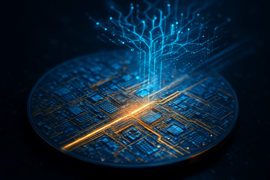
The Technical Leap: Superpower Rail and the 1.6 Nm Frontier
The A16 process marks TSMC’s entry into Angstrom-scale technology, employing an enhanced gate-all-around (GAA) nanosheet transistor. While the previous two nm (N2) node introduced GAAFETs, the A16 introduces the Super Power Rail, an advanced backside power delivery network that relocates power circuits beneath the silicon wafer. Unlike Intel’s PowerVia approach, TSMC’s SPR supplies power directly to the source and drain of each transistor.
The direct contact method is more difficult to manufacture, but it offers significant electrical improvements by relocating power delivery to the back and keeping signal routing on the front. SPR eliminates routing congestion common in dense AI chips. A16 delivers 8 to 10% higher clock speeds at the same voltage and reduces power use by 15 to 20% compared to the N2P (2 nm enhanced) node. Logic density increases by 1.1 times, enabling more processing cores within the same footprint.
Initial reactions from the semiconductor research community have been highly favorable, though some experts note the immense manufacturing hurdles. Moving power to the backside requires advanced wafer bonding and thinning technologies, techniques that must be executed with atomic-level precision. However, TSMC’s decision to stick with existing extreme ultraviolet (EUV) lithography tools for the initial A16 ramp, rather than immediately jumping to the more expensive High NA EUV machines, suggests an intentional strategy to maintain high yields while providing cutting-edge performance.
The AI Gold Rush: NVIDIA, OpenAI, and the Battle for Capacity
The A16 roadmap announcement has triggered a rush among top tech companies. NVIDIA, a leader in AI data centers, has reportedly secured early exclusive access to A16 for its 2027 Feynman GPU. For Nvidia, the 20% power savings from A16 is a key advantage, especially as data centers work to manage the heat and power needs of large H100 and Blackwell clusters.
In a surprising strategic shift, OpenAI has also emerged as a key stakeholder in the A16 era, working alongside partners such as Broadcom and Marvell. OpenAI is reportedly developing its own custom silicon and an Extreme Processing Unit (XPU) optimized for its GPT-5 and Sora models. Using TSMC’s A16 node, OpenAI seeks to achieve a level of vertical integration that could eventually reduce its reliance on off-the-shelf hardware. Meanwhile, Apple, traditionally TSMC’s largest customer, is expected to use A16 for its 2027 M6 and A21 chips, ensuring its edge AI capabilities remain ahead of the competition.
The competitive implications reach beyond chip designers to other foundries. Intel, which has been vocal about its five-node-in-four-years strategy, is currently shipping its 18A node with PowerVia technology. While Intel reached the market first with backside power, TSMC’s A16 is widely viewed as a more refined and efficient implementation. Samsung has also faced challenges, with reports showing that its 3nm GAA yields have trailed TSMC’s, leading some customers to migrate their 2026 and 2027 orders to the Taiwanese giant.
Wider Significance: Energy Geopolitics and Scaling Principles
The move to A16 and the Angstrom era has big effects on the wider AI world. By late 2025, AI data centers are expected to use almost half of all data center electricity worldwide. The efficiency gains from Super Power rail technology are not only a technical upgrade but also needed for economic and environmental reasons. For large companies like Microsoft and Meta, adopting A16 chips could save billions of dollars each year by reducing cooling and electricity costs.
This development also underscores the semiconductor supply chain’s importance to global politics. TSMC’s market value hit a record $1.5 trillion in late 2025, underscoring its role as the foundry utility of the global economy. Still, having so much key technology in Taiwan is a strategic worry. To address this, TSMC is accelerating equipment upgrades in Arizona and Japan and aims to start A16 production in the US by 2028 to meet security needs for American AI labs.
Compared to earlier milestones such as FinFET-to-GAAFET, A16 marks a technical shift. The industry priority is shifting from scaling for smaller features to architectural intelligence. Instead of focusing on transistor count increases (as in Moore’s Law), system-on-wafer scaling is now central. The methods for building, powering, and interconnecting chips are as technically crucial as transistor size.
The Road to Sub-1nm: What Lies Beyond A16?
Looking forward, the A16 node is just the start of the Angstrom era. TSMC is researching the A14 (1.4 nm) and A10 (1 nm) nodes targeting a launch in the late 2020s. These nodes are expected to employ new channel materials, such as two-dimensional semiconductors and molybdenum disulfide (MoS2), to overcome silicon’s scaling limits.
In the short term, the industry will watch TSMC’s N2 node ramp in 2025. This will signal how well A16 might do. If TSMC keeps its usual yield rates with GAA FETs, moving to A16 and Super Power Rail in 2026 should go smoothly. Still, there are challenges, especially with packaging. As chips become more complex, advanced 3D packaging, such as CoWoS (chip-on-wafer-on-substrate), will be required. This packaging connects A16 chips to high bandwidth memory (HBM4), which could slow down the supply chain.
Experts believe the A16’s success will open the door to new AI applications that were once too costly to run. This could mean real-time, high-quality video generation and autonomous agents capable of managing complex multi-step tasks. As hardware gets more efficient, the cost of running AI models or inference will fall, making advanced AI common in consumer electronics and industrial automation.
Summary and Final Thoughts
TTSMC’s A16 and Super Power Rail Technology signal a major advance for AI. By moving power delivery to the wafer’s back and reaching 1.6 nm, TSMC provides the thermal and electrical capacity critical for rapid AI growth. With mass production expected in late 2026, A16 is set to propel the next wave of AI innovation.
For investors, the message is clear: new chip designs now drive the semiconductor industry. While Intel and Samsung are progressing, TSMC leads with its Angstrom roadmap, making it the top choice for AI companies. The coming yield reports from the 2 nm ramp will indicate if TSMC remains on track for A16.
Source: TSMC’s A16 Roadmap: The Angstrom Era and the Breakthrough of Super Power Rail Technology