


Santa Clara, California
Intel has given control of one of its most important manufacturing areas to someone who previously led the world’s second-largest memory company. This move reveals more about the future of enterprise computing than any product roadmap could.
On June 18, 2026, Intel announced that Seok-Hee Lee will become executive vice president of Intel Foundry, reporting directly to CEO Lip-Bu Tan. This Intel Foundry leadership appointment is more than a routine leadership change. Intel is making advanced packaging systems a separate, dedicated business unit. This shows that the way chips are assembled is now just as important as the chips themselves.
The Intel Foundry Leadership Appointment That Signals a Structural Pivot
For many years, the semiconductor industry viewed packaging as an afterthought; the last step after the main engineering work was complete. That view no longer applies.
Intel is making advanced packaging systems a focused business with its own leadership. This reflects how important and complex packaging has become for performance, power efficiency, and the integration of different technologies in AI systems. Lee will oversee everything on the back end, including system integration, technology development, and mass production. This is a broad role and acts as a second command center within Intel Foundry.
Now that Lee is in charge of back-end operations, Naga Chandrasekaran will focus on front-end work for Intel’s 18A and 14A process nodes. This split is intentional. Intel now manages front-end silicon fabrication and back-end module assembly as separate, parallel tracks, each having its own executive leader. This approach is similar to how aerospace or automotive companies separate engine engineering from final vehicle assembly. The complexity of the work requires this structure.
Why Seok-Hee Lee, and Why Now?
Lee’s background is no coincidence. He worked at Intel for about 10 years early in his career, then held leadership roles in the Korean chip industry, including serving as CEO of SK hynix, one of the world’s two largest high-bandwidth memory suppliers. High-bandwidth memory, which is stacked DRAM used in AI data centers, is itself a product of advanced packaging systems. Lee has direct experience with the manufacturing challenges that Intel now wants to handle on a larger scale.
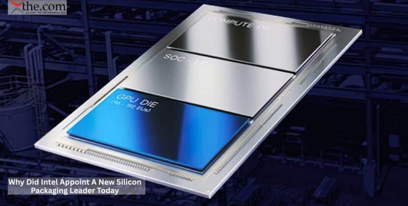
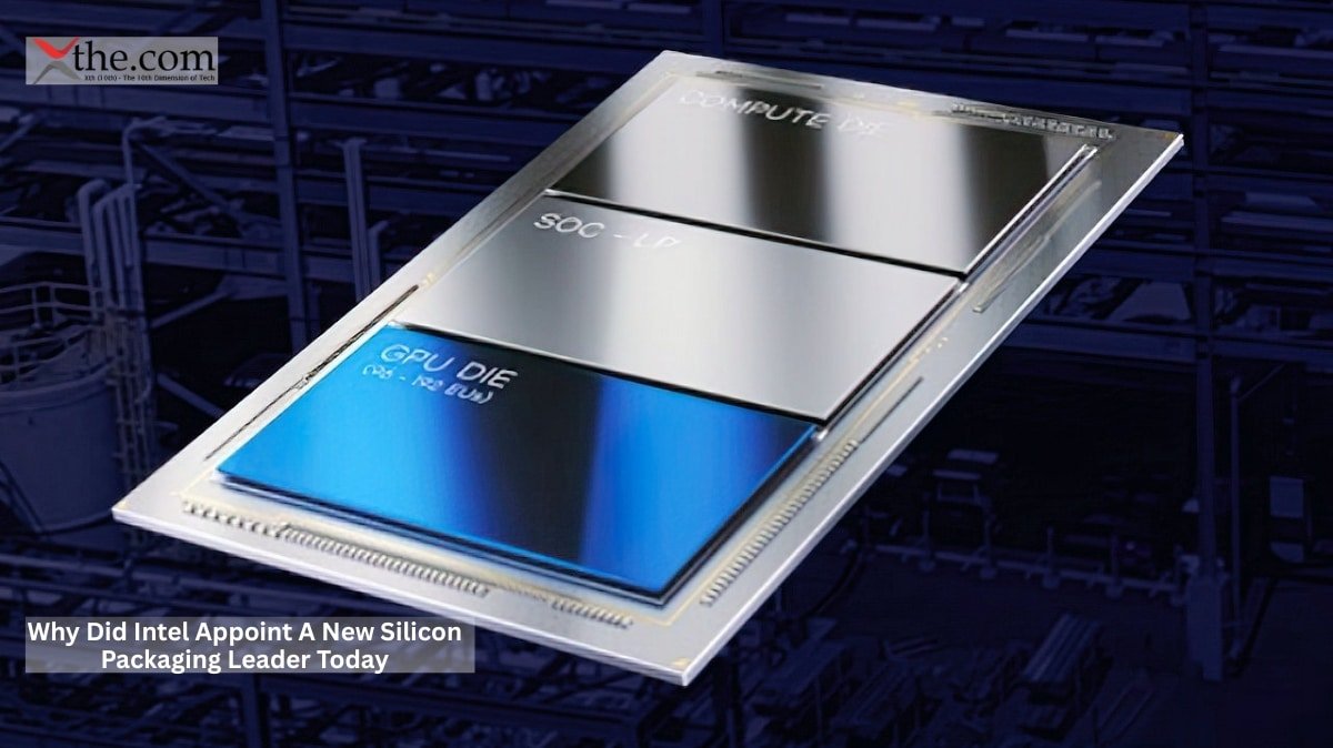
CEO Lip-Bu Tan explained that the appointment addresses a specific need: bringing together advanced logic, memory, networking, and other parts to build high-performance systems for Intel Foundry customers. Intel plans to use EMIB-T and HBI packaging technologies on a larger scale. EMIB, or Embedded Multi-die Interconnect Bridge, lets Intel connect different silicon dies using a small bridge in the package. HBI, or Hybrid Bonding Interconnect, increases density by replacing traditional solder bumps with direct copper-to-copper connections. Both technologies are central to chip manufacturing at the density levels AI accelerators now demand.
Logic Modular Integration: The Engineering Bet Behind the Org Chart
At its core, Intel’s restructuring is about logic modular integration. This means you can achieve performance improvements similar to shrinking a process node simply by improving how separate dies communicate over shorter, faster connections.
For an enterprise network builder setting up server racks for large-language-model inference, this change is significant. A single high-performance module with tight logic modular integration, where the CPU, HBM memory stack, and network interface are all in one compact package, can replace what used to require several separate components on a circuit board. This leads to fewer connections, lower latency, and less power used for signals.
Chip manufacturing has traditionally been the story of transistor density cramming more switching elements onto a given area of silicon. The physics of that race, governed by atomic-scale lithography limits, is progressively harder to win. Advanced packaging systems offer an orthogonal path: instead of shrinking individual dies further, you assemble multiple specialized dies into a single module so tightly coupled that it behaves like a monolithic chip. The Intel Foundry leadership appointment advanced packaging systems strategy Lee now leads is a direct institutional devotion to that alternative trajectory.
The Domestic Supply Chain Dimension
American hardware developers, whether in Austin or Seattle, have a practical concern beyond engineering: where will these modules be made?
This appointment comes as Intel’s U.S. manufacturing operations are gaining new momentum. Intel already has back-end facilities in Chandler, Arizona, and has made expanding domestic chip manufacturing a top priority, especially with continuing geopolitical concerns about Asian supply chains. Having a dedicated business unit for advanced packaging systems with its own leader makes it easier to attract U.S. government investment, negotiate contracts that require domestic assembly, and hold one person accountable for meeting deadlines.
Intel has also signed Tesla as the first major customer for its new 14A manufacturing process. This shows that American industrial customers are ready to support Intel’s plans if the company can meet its promises. Lee’s appointment is meant to help build that trust, especially in back-end operations, where earlier delays in logic modular integration have made it hard for Intel to compete with TSMC’s CoWoS packaging for AI chips.
What Navid Shahriari’s Departure Means
Intel also shared that executive vice president Navid Shahriari will retire after 37 years at the company. Shahriari’s long career covered many phases of Intel’s manufacturing history. His retirement, coinciding with this restructuring, signals a clear shift away from the days when chip manufacturing and packaging were managed together. The new structure recognizes that both areas have become too complex and distinct to be handled as a single group.
The Stakes for Enterprise Hardware Builders
The Intel Foundry leadership appointment advanced packaging systems bifurcation will take years to fully validate. High-volume ramp of EMIB-T and HBI involves yield management challenges that even well-resourced manufacturers have struggled with. TSMC and Samsung are not standing still.
Still, Intel has made a serious structural commitment. A dedicated business unit is held to different standards than a program hidden within a larger organization. Lee will now be closely watched each quarter for back-end yield rates, packaging cycle times, and the delivery of customer orders something his predecessor did not face.
For data center architects and network infrastructure leaders planning long-term purchases, the main question is not whether Intel’s advanced packaging systems strategy makes sense it does. The real question is whether Intel now has the organization in place to make it happen. As of June 18, 2026, Intel has officially decided that it must.
The next public test of Intel’s commitment will be when the company announces its first volume shipments of EMIB-T to external Foundry customers. This milestone will show whether the new leadership appointment leads to real results or just a more organized company chart.
Source: Intel Announces Leadership Appointment at Intel Foundry to Accelerate Development and Manufacturing