Key Takeaways 

  • New AWS Graviton5-based Amazon EC2 M9G instances deliver up to 25% higher performance than the previous generation.  
  • Each chip features 192 cores and a larger cache, enabling bigger workloads, improved application performance, and lower costs.  
  • For the 3rd year in a row, over half of the new CPU capacity added to AWS uses Graviton. In fact, 98% of the top 100-1000 EC2 customers, including Adobe, Airbnb, Altacn, Epic Games, F1, Pinterest, SAP, Siemens, Snowflake, and Synopsys, are already seeing the price and performance benefits of Graviton.  

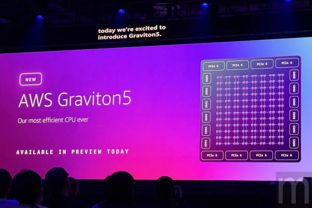
As cloud workloads become more complex and larger, organizations commonly struggle to deliver faster performance, lower costs, and meet eco-friendly targets simultaneously. Traditional solutions usually require compromises between speed and capability. To solve this, we are introducing Graviton 5 processors, AWS’s most advanced chip yet, for a wide range of cloud workloads. Graviton 5 delivers up to 25% better compute performance than the previous generation while keeping energy use low, so you can run applications faster, save money, and support your sustainability targets.  

Graviton 5 Delivers Measurable Business Impact 

Graviton 5-based M9G instances process data faster with 192 CPU cores, reducing inter-core latency and boosting bandwidth for demanding workloads such as gaming analytics and server workloads.  

The chip includes a 5x larger L3 cache and a high-speed memory buffer that keeps frequently accessed data close to the processor. Each Graviton 5 core has 2.6x the L3 cache of Graviton 4, resulting in fewer delays waiting for data and faster application response times. Memory performance has also improved with Graviton 5, yielding faster memory speeds that enable you to process larger data sets and run memory-intensive applications more efficiently.  

Network and storage bandwidth are higher, improving data transfer, backups, and distributed app performance.  

Graviton 5 delivers better performance and consumes less energy, so you can meet your eco-friendly targets without sacrificing performance. These improvements come from AWS controlling everything from chip design to server architecture. Graviton 5 uses the latest 3NM technology, is optimized for AWS needs, and supports system-level improvements such as bare-die cooling.  

Graviton 5 Advances Security Without Compromise 

Built in the AWS Nitro system, Graviton 5 uses dedicated hardware for security, ensuring resources are focused on your workloads and access is restricted.  

Graviton 5 introduces the Nitro Isolation Engine, an advancement to the Nitro system that harbors formal verification to provide mathematical certainty that your workloads are isolated from each other and from AWS operators. NGIN’s minimal, formally verified codebase uses mathematical proofs to ensure it behaves exactly as defined, pioneering a new standard for mathematically proven cloud security. We will engage with customers to provide access to the Nitro Isolation Engine implementation so they can evaluate it and the resulting proofs.  

Customers In Many Industries Have Seen Strong Results 

  • Adobe uses Graviton to deliver customized viewing for millions, leveraging greater compute power to process video streams and real-time Epic Games. It depends on Graviton to deliver smooth, competitive gaming to millions of players every day, even during peak demand.  
  • Formula 1 relies on Graviton to quickly process telemetry data and deliver timely live race updates to fans, improving the quality and speed of fan engagement during events.  
  • Pinterest relies on Graviton-based systems to serve over 500 million monthly users. With Graviton’s custom performance benefits, they deliver personalized content more efficiently at scale, helping Pinterest maintain a positive user experience and strong platform reliability.  

Expanding for Airbnb, started in 2007 when two hosts welcomed three guests into their co-house. Today, it has over five million hosts and more than two billion guest arrivals worldwide. AWS’s Graviton-based Amazon EC2 (Elastic Compute Cloud) instances, which are virtual servers in the AWS Cloud, are among the fastest EC2 instances we have ever tested, Dennis Sheahan, principal performance engineer at Airbnb, said. In our performance tests performed using Airbnb’s production search workloads, we are seeing improvements of up to 25% over other system architectures of the same generation and up to 20% compared to prior-generation Graviton 4 instances. Especially impressed with P95 latency (the time taken for 95% of search requests to complete) for our critical workloads, helping to provide a consistent experience for Airbnb guests and hosts.  

Atlassian, a leader in software development and work management, helps businesses connect teams and boost productivity with AI-powered tools. Paolo Almeida, Principal Site Reliability Engineer at Atlassian, notes that moving Jira to Graviton 5-based M9G instances has delivered 30% higher performance and 20% lower latency than the previous generation, resulting in faster, more efficient experiences for end users of Atlassian’s cloud tools.  

Siemens Digital Industries Software helps organizations of all sizes go digital with software, hardware, and services from the Siemens Xcelerator platform. Siemens Calibre Design Solutions offers a full platform for integrated circuit verification and manufacturing design. The future of semiconductor physical verification lies in cloud-enabled high-performance computing, says Juan Rey, senior vice president and general manager at Siemens Digital Industries Software. Our alliance with AWS positions Calibre at the leading edge of this transformation. We’re excited to announce support for Calibre on Arm-based AWS Graviton processors, which deliver 20% performance improvements and more than 30% reduction in compute costs on AWS Graviton compared with other AWS instances. Early AWS Graviton 5 testing shows an additional 30% boost, unlocking faster verification and shorter time-to-market for our customers.  

For over 50 years, organizations have trusted SAP to bring out their best by uniting business-critical operations across finance, procurement, HR, supply chain, and customer experience. We’ve been working closely with AWS on running SAP and cloud on AWS Graviton since 2023 and have seen notable performance enhancements with each new Graviton generation, said Stefan Bauerle, Senior Vice President and Head of SAP HANA and persistence at SAP. With AWS Graviton 5-based Amazon EC2 M9G instances, we’ve observed a stunning 35% to 60% increase in the performance of our OLTP queries on SAP HANA cloud. A phenomenal progress in a single day. Generation  

Synopsys leads in engineering solutions from silicon to systems, helping customers quickly develop AI-powered products for over a decade. Since the inception of Annapurna Labs, Synopsys and AWS have collaborated to enable Amazon’s custom silicon development, said Sanjay Bali, senior vice president in strategy and product management at Synopsys. Synopsys EDA tools, such as VCS, PrimeTime, Fusion Compiler, and IC wild data support, run on AWS Graviton and have been critical to the design of the Graviton, Nitro, and Titanium chips. Today, Synopsys and AWS are expanding Graviton to accelerate our customers’ semiconductor innovation. Early results on Graviton 5 show up to 35% runtime gains for Fusion Compiler and PrimeTime. Our joint partner ARM reports up to 40% faster run times for Synopsys VCS on Graviton 5 compared to previous generations.  

Graviton 5-based M9G instances designed for general-purpose workloads are now available in preview. C9G instances for compute-intensive workloads and R9G instances for memory-intensive workloads are planned for 2026.

Source: AWS introduces Graviton5: the company’s most powerful and efficient CPU 

Apple has introduced the M5 chip, which brings major improvements in AI performance and upgrades across almost every part of the chip. Built with third-generation 3nm technology, the M5 features a new 10-core GPU design with a neural accelerator in each core. This setup lets AI tasks run much faster, offering 4x the peak GPU compute performance of the M4. The GPU also offers better graphics capabilities and third-generation ray tracing, which together boost graphics performance by up to 45% compared to the M4.  

Claiming the title of world’s fastest performance core, the M5’s CPU flexes up to 10 cores six built for efficiency, four for performance. This powerful blend delivers up to 15% faster multi-threaded performance than the M4. The chip is packed with a turbocharged 16-core neural engine and a robust media engine, plus nearly 30% more unified memory bandwidth, peaking at 153 GB. This all-star performance now fuels the 14-inch MacBook Pro, iPad Pro, and Apple Vision Pro each ready for the spotlight and available to pre-order now.  

M5 ushers in the next significant step in AI performance for Apple’s silicon, said Johny Srouji, Apple’s Senior Vice President of Hardware Technologies. With the introduction of neural accelerators in GPUs, M5 delivers a significant boost to AI workloads. Combined with a significant increase in graphics performance, the world’s fastest CPU core, a faster neural engine, and even higher unified memory bandwidth, M5 delivers far greater performance and capabilities across MacBook Pro, iPad Pro, and Apple Vision Pro.  

A New GPU Architecture Designed For AI And Graphics 

The M5’s cutting-edge GPU architecture is crafted to put AI front and center. Each of its ten GPU cores features a neural accelerator, sprinting ahead with over four times the peak GPU compute of M4 and more than six times the AI muscle of M1. With M5, the new 14″ MacBook Pro and iPad Pro conquer AI-driven tasks in record time, whether running diffusion models in creative apps like Draw Things or processing massive language models right on your device. Explore new creative heights with platforms such as WebAI.  

The M5’s new GPU and improved shader cores boost graphics performance by up to 30% over the M4 and up to 2.5 times over the M1. The chip also features Apple’s third-generation Ray Tracing engine, which can increase graphics performance by up to 45% in apps that use Ray Tracing, thanks to redesigned dynamic caching. The GPU delivers more fluid gameplay, more realistic 3D visuals, and faster rendering for graphics projects. On the Apple Vision Pro, the M5 follows the micro OLED displays to show 10% more pixels and supports refresh rates up to 120 Hz, making images sharper, motion smoother, and reducing blur.  

The GPU architecture is designed for effortless integration with Apple’s software frameworks. Applications that use built-in Apple frameworks and APIs such as Core ML, Metal Performance Shaders, and Metal 4 can achieve immediate performance gains. Developers can also build solutions for their apps by directly programming the neural accelerators using Tensor APIs in Metal 4.  

A Faster Neural Engine for Smarter Features 

The faster 16-core Neural Engine delivers powerful AI performance with incredible energy efficiency, complementing the neural accelerators in the CPU and GPU to make M5 fully optimized for AI workloads. For example, AI-powered features on Apple Vision Pro, like the ability to transform 2D photos into spatial scenes in the Photos app or generate a persona, operate at greater speed and with greater capability.  

The Neural Engine in the M5 chip boosts performance for Apple intelligence on-device AI tools, such as Image Playground, which run faster, and Apple intelligence models work better thanks to the improved Neural Engine and unified memory in M5. Developers using Apple’s Core ML models framework will also see faster results.  

More Memory Means More AI Power 

The M5 chip has a unified memory bandwidth of 153 GB/s, which is almost 30% more than M4 and over twice that of M1. Its unified memory lets the entire chip use a single large pool of memory, so devices like the MacBook Pro, iPad Pro, and Apple Vision Pro can run larger AI models right on the device. This memory also powers the faster CPU, GPU, and Neural Engine, giving you better performance in apps, smoother graphics in creative tools and games, and quicker AI tasks with up to 32 GB of memory. M5 lets you run demanding apps like Adobe Photoshop and Final Cut Pro simultaneously, even while uploading large files to the cloud.  

Apple Silicon’s Impact on the Environment 

Apple 2030 is the company’s ambitious plan to be carbon neutral across its entire footprint by the end of this decade, by reducing product emissions from its three biggest sources:  

  • Materials  
  • Electricity  
  • Transportation  

The power-efficient performance of M5 helps the new 14-inch MacBook Pro, iPad Pro, and Apple Vision Pro meet Apple’s high energy-efficiency standards and reduce total energy consumption over the products’ lifetimes.

Source: Apple unleashes M5, the next big leap in AI performance for Apple silicon 

TSMC’s 2nm (N2) production is fully booked through 2026, mainly due to strong demand for AI chips and new mobile processors. This high demand has led TSMC to accelerate production, and 2nm revenue is expected to surpass that of 5nm and 3nm by the third quarter of 2026.  

Main Details of 2NM Demand and Capacity 

  • TSMC’s first two 2nm factories, Fab 20 in Hsinchu and Fab 22 in Kaohsiung, are fully booked for all of 2026.  
  • TSMC started large-scale 2NM production in the fourth quarter of 2025, with reported yields of about 70%.  
  • Capacity expansion: TSMC plans to increase its 2NM monthly production capacity to 90,000-100,000 wafers by 2026. To handle the demand, 10 total 2NM facilities are planned across Taiwan and the U.S., with some reports indicating capacity could reach 140,000 wafers per month by the end of 2026.  
  • Major customers: Apple has secured more than 50% of the initial 2nm capacity for its future A20 and M6 chips. Other major clients lining up for 2nm include N Media, AMD, Qualcomm, and Mediatek.  
  • Because demand is so high, TSMC can charge more with TS2NM wafers expected to cost about $30,000 each.  

AI And 2Nm Technology 

The 2NM node is key for AI development, offering a 10% to 15% performance boost or a 25% to 30% reduction in power consumption compared to the 3NM process. This efficiency remains critical for AI data centers and high-performance computing (HPC).  

  • The fact that 2NM production is overbooked shows that the AI infrastructure cycle is growing mainly because AI models are using more tokens.  
  • N2 vs 3Nm: Demand for 2Nm is expected to surpass that for 3Nm as 2Nm technology is considered more cost-efficient for advanced AI products despite its higher base price.  

Future Outlook 

  • By 2027, TSMC’s 2NM capacity is expected to grow between 160,000 and 180,000 wafers per month.  
  • A more advanced 2NM process called N2P is expected in 2026. The next generation 1.6NM (A16) chip is planned for late 2026 or early 2027.  
  • Competition has been prolonged, while Samsung has started 2nm GAA (gate-all-around) production, TSMC currently holds the dominant position in the high-volume, high-end market due to higher yields.  

TSMC’s US$28.6 billion investment in 2nm capacity underlines its strategy to remain the preferred supplier for leading AI companies seeking high-performance chips.  

As 2025 wraps up, the 3nm era may be coming to an end, too. In 2026, the 2nm era could begin, with Apple reportedly leading the way for its A20 and A20 projects. TSMC is at the center of this shift, using the Gate-All-Around (GAA) Architecture. TSMC aims to boost both performance and effectiveness for its 2nm node. This has attracted many clients to the new process. According to a recent report, TSMC’s 2nm capacity for 2026 is already fully booked.  

TSMC’s 2NM capacity is fully booked until the end of 2026. 

Earlier reports noted that two of the tech giants’ two NM plants were already full, requiring the company to start three additional production facilities to meet overwhelming demand. This apparently requires an estimated investment of $28.6 billion. The United Daily News reports that TSMC’s entire 2NM process is fully booked until the end of 2026. The mass production could start as early as the end of the year.  

Qualcomm, MediaTek, Apple, AMD, and others are eager to use the 2nm process. Reports say Apple has secured over half of the initial capacity to gain an edge over competitors.  

Apple has reportedly secured over half of TSMC’s initial 2nm output. TSMC aims to increase monthly output to 100,000 units by the end of 2026. GAA offers advantages over FinFET with nano-sheet stacking, improving current control and reducing leakage. The 2nm process can boost performance by 10 to 15% at the same power or cut power by 25 to 30% at fixed performance.  

Samsung has also started mass production of its 2nm GAA process. So far, the results show only small improvements in performance and power efficiency compared to 3nm, but these numbers may improve over time. TSMC forecasts predict its capital spending in 2026 could reach $48-50 billion, setting a new record.  

TSMC is ramping up 2NM chip production for 2026, marking a major advance in chip technology. Volume production began in the fourth quarter of 2025. Early yields are strong, with reports of about 70% and even over 90% for some memory products. This progress is significant for the semiconductor industry and leading tech companies. Higher output and broader market availability are expected in 2026.

Source: TSMC’s 2nm Chip Production Capacity Already Booked Through 2026 

On January 27, 2026, the semiconductor industry saw its biggest shift in a decade. Intel Corporation announced that its 18A-class manufacturing mode is in high-volume production, achieving its goal of introducing five new manufacturing modes in four years. This is more than a technical win. It marks Intel’s return to process leadership, a position lost in the late 2010s.  

The Intel 18A launch is a major moment for artificial intelligence. By combining the Ribbon-FIT get-all-around (GAA) design with back-side power delivery, Intel has created a platform for the next generation. A wave of Generative AI and High Performance Computing. Early versions are already shipping to key customers, and 18a is quickly becoming the top choice for AI developers seeking the best performance per watt as energy costs rise.  

The Architecture of Leadership: RibbonFet and the PowerVia Advantage 

Intel 18A stands out because of two major innovations: Ribbon-FET, which is Intel’s name for a type of Gate All Around (GAA) transistor that improves current control and reduces power loss, and PowerVia, a new approach to supplying power.  

Unlike the older Fin-FET design, which used a vertical fin to manage current, Ribbon-FET wraps the transistor channel on all four sides. This gives better control over electrical leakage and much faster switching speeds. The 18A node improves on the Ribbon-FET design. First seen in the 20A node, delivering a 10-15% speed increase at the same power as the 20A node.   

The second and perhaps more consequential breakthrough is PowerVia Intel’s implementation of Backside Power Delivery (BSPDN). Traditionally, power and signal wires are bundled together on the front of the silicon wafer, leading to routing congestion and voltage droop. PowerVia moves the power-delivery network to the backside of the wafer using Nano-TSVs (through-silicon vias) to connect directly to transistors. This decoupling of power and signal allows for much thicker, more efficient power traces, reducing resistance and reclaiming nearly 10% of previously wasted dark silicon area.  

While competitors like TSMC have announced their own version of this technology, called SuperPower Rail, for their upcoming A16 node, Intel launched its version almost a year earlier. This early lead in back-side power delivery is a key reason for the A18a node’s strong performance. Industry analysts say the A18a node delivers a 25% improvement in performance per watt over the Intel 3.0 Node-A, changing the competitive landscape for chip foundries.  

The successful ramp of 18A has caused shockwaves through the tech giant ecosystem. Intel Foundry has successfully launched 18A, which has made a big impact among major tech companies. Intel Foundry now has a backlog of over $20B with Microsoft as a leading customer. Microsoft is using the 18A-P (performance-enhanced) version to build its next-generation MAIA-II AI accelerators. By using Intel’s factories in Arizona and Ohio, Microsoft gains a performance advantage and also protects its supply chain from risks in East Asia.  

Reports from late 2025 indicate that Apple has more than a portion of its silicon production for entry-level purchases to Intel’s 18A/P node. This is a historic diversification for Apple, which has consistently relied almost exclusively on TSMC for its A series and M series chips. For Intel, winning an Apple-sized contract validates the maturity of its 18A process. It proves Intel can meet the stringent yield and quality requirements of the world’s most demanding hardware company.  

For AI hardware startups and big players like NVIDIA, access to 18A offers an important option. In a market where supply is tight, NVIDIA still mainly works with TSMC; however, Intel’s 18A-PT is designed for Advanced Multi-Die System-on-Chip SOC designs and could be a strong choice for future Blackwell chips. Intel’s Foveros Direct 3D Packaging lets companies stack high-performance 18A logic tiles. This approach is a major advantage, as everyone races to build the first 100-trillion-parameter AI models.  

Geopolitics and the Re-Shoring of the Silicon Frontier 

Intel 18A is more than a technical achievement; it plays a key role in bringing semiconductor manufacturing back to the United States, thanks to the CHIPS and Science Act. Intel’s expansion of Fab 52 in Arizona acts as a sign of renewal for American industry. The 18A node is the first advanced process in over 10 years to be developed and mass-produced in the U.S., before anything else, with big implications for national security and technology independence.  

The success of 18a also proves that Intel’s five-nodes-in-four-years strategy is working, as it moves quickly. Intel has jumped ahead of the usual industry pace and pushed competitors to speed up their own plans. This rapid progress is important for AI, where computing power doubles every few months. With improvements enabled by technologies like PowerVia and Ribbon-FET, running large AI data centers would likely become too expensive.  

The transition has always raised concerns. The immense capital expenditure needed to maintain this space has pressured Intel’s margins. The complexity of 18A manufacturing demands a highly specialized workforce. Observers initially doubted Intel could achieve commercial yields (currently estimated at a healthy 65-75%). The successful launch of the Panther Lake consumer CPUs and Clearwater Forest Xeon processors has largely silenced skeptics.  

The Road to 14A and the Era of High NA EUV 

Looking ahead, 18A is only the start of Intel’s angstrom-era plans. Intel has already started testing its next-generation 14A node. This will be the first in the industry to use ASML’s high-numerical-aperture (high NA) extreme ultraviolet (EUV) lithography tools. HiNA refers to a lithography lens with greater light-gathering capability, enabling more precise patterning, while EUV is a technology that uses short-wavelength light to create smaller circuit features. 18A helps Intel catch up with 14A. AMS to push even further, it will offer another 15% performance boost along with even smaller features.  

The embedding of A18a technology into the Nova Lake architecture, scheduled for late 2026, will be the next major milestone for the consumer market. Experts predict that Nova Lake will reinvent the desktop and mobile computing experience by offering over 50 TOPs of NPU performance, effectively making every 18A-powered PC an AI-localized AI powerhouse. The challenge for Intel will be to preserve this momentum while simultaneously scaling its foundry services to support a diverse range of third-party designs.  

A Fresh Chapter for the Semiconductor Industry 

The high-volume manufacturing of A18a marks one of the most remarkable corporate turnarounds in recent history. It delivers 10-15% speed gains and pioneers backside power delivery via PowerVia. Intel has not only caught up to the leading edge but has actively set the pace for the rest of the decade. This development ensures the AI revolution will have the silicon fuel it needs to sustain its exponential growth.  

As 2026 approaches, everyone in the country will be watching how the first A18a devices perform in stores. There is also interest in how Intel Foundry’s customer base grows. The Angstrom race is still ongoing. Now that A18a is in production, Intel has clearly regained its place as an authority in the chip world. For the first time in a generation, the fastest and most efficient transistors are being made by the company that began it all. 

SourceIntel Reclaims Silicon Crown: 18A Process Hits High-Volume Production as ‘PowerVia’ Reshapes the AI Landscape 

By March 2026, global AI focus has shifted from raw power to localized control. Fast, centralized AI development is giving way to a regulated, fragmented model called Sovereign AI. Google Cloud leads with sixth-generation TPU v6 Pods, enabling new Regional Sovereign AI Hubs across Europe, Asia, and Latin America. 

For enterprise architects and government agencies, this change is more than just hardware updates. It means a complete redesign of the AI infrastructure. It combines the high performance of the Trillium architecture with strict national data security needs. 

The Architecture: Why TPU v6 (Trillium) is the Sovereign Engine 

The TPU v6, referred to internally at Google as Trillium, is their biggest advance in ASIC design to date. While the earlier v5p was built for large-scale LLM training in massive regional pods, the v6 is redesigned to be more efficient at regional hubs and supports multiple organizations with strong data separation. 

1. The Systolic Array Expansion 

The TPU v6 features a larger design. Google has doubled the Matdoubltiply Unit (MXU) size from 128×128 to 256×256, which means four times as many FLOPs per cycle at the same speed. This lets regional hubs handle large datasets using less space, providing the high-speed “workspace” necessary to run trillion-parameter models locally. The Inter-Chip Interconnect (ICI) has been boosted to 1.2 TBps, enabling a single TPU v6 Pod consisting of 256 interconnected chips to act as a unified, 235-petaflop “supercomputer in a box.”  

The Rise of Sovereign AI Hubs 

Digital sovereignty means that a nation’s data and AI models must comply with its own laws. They must also be safe from foreign control or outside surveillance. Google’s rollout of TPU v6 Pods in regional hubs, like the new Munich Sovereign Cloud Hub, and soon in Brazil, Sweden, and Saudi Arabia, supports three key areas: 

Pillar 1: Data Residency and “Air-Gapped” Operation 

For the first time, Google is offering Google Cloud Air-Gapped solutions powered by TPU v6. In these environments, the hardware operates without a physical connection to the public internet or the global Google backbone. This is essential for the defense, intelligence, and national healthcare sectors, which cannot risk metadata leakage to US-based servers.  

Pillar 2: Administrative Oversight 

Google teams up with local ‘sovereign operators’ like S3NS in France. Workspace by STACKIT in Germany is another partner. These groups grant operational control to local staff with national security clearance. They run the TPU v6 Pods and ensure encryption keys and access records stay within the country. 

Pillar 3: Model Autonomy 

Regional hubs are designed to host Localized LLMs. Rather than sending data to a global Gemini endpoint, enterprises can fine-tune “Sovereign Gemini” or open models like Gemma 2 directly on local TPU v6 hardware. This ensures that a nation’s AI weights and training data remain a domestic asset.  

Performance Metrics: Regional Efficiency 

The TPU v6 Pod deployment isn’t just about security. The TPU v6 Pod rollout is not only about security, but also about energy efficiency. Google says the v6 delivers up to 4.7 times the peak compute performance per watt compared to the v5e. Since energy constraints are a major challenge for data centers, this efficiency helps regional hubs operate within the power limits of cities in Europe and Asia. 

Metric TPU v5p (2024) TPU v6 Trillium (2026) Generation Jump 
Peak BF16 Compute 459 TFLOPs 1,200+ TFLOPs ~2.6x 
HBM Capacity 95 GB 192 GB 2x 
ICI Bandwidth 4,800 Gbps 1.2 TBps 2.5x 
Energy Efficiency Base +67% vs v5e Significant 

In Germany, T-Systems and Google Cloud work together as a model for TPU v6 deployment. They deploy Pods in T-Systems’ Frankfurt facilities. Now, German public agencies can use the Vertex AI stack to modernize tax platforms and national ID systems. They do this without breaking the EU Cloud Sovereignty Framework.  

These agencies use the v6 Pod’s built-in Int4/Int8 support to enable real-time agentic workflows. For example, a local workflow can now handle millions of social benefit applications, checking for fraud and compliance within Germany’s legal limits and reducing processing times from weeks to seconds. 

Strategic Action Items for IT Leaders 

If your organization must comply with residency rules such as GDPR, India’s Digital India mission, or Brazil’s LGPD, the new TPU v6 regional pods will change your technology planning. 

  1. Audit data boundaries. Figure out which workloads need ‘Dedicated’ or ‘Air-Gapped’ infrastructure. TPU v6 works for both, but ‘Air-Gapped’ setups cost more to run. 
  1. Evaluate “Agentic” readiness. Use this week to test Gemini Enterprise features in a regional preview. The v6’s lower latency for “long-context” reasoning makes it ideal for autonomous agents. These agents must operate in complex, localized, regulatory environments.  
  1. Plan for Portability: Ensure your AI models are built using open frameworks like JAX. Plan for Portability: Build your AI models using open-source frameworks such as JAX, PyTorch/XLA, or TensorFlow. This way, you can move your workloads between global and sovereign hubs as rules change.ty was equated with isolation using inferior local tech to stay safe. Google’s TPU v6 deployment proves that a nation can have hyperscale powerwhile maintaining local control. As these Pods continue to roll out through the remainder of 2026, the question is no longer whether you can afford to use AI, but whether you can afford to use AI that isn’t sovereign.

Source: Technology 

NVIDIA is said to be working on an open-source AI platform called NemoClaw. This platform is meant to make it easier and safer for companies to use autonomous AI agents. NVIDIA plans to introduce Nemoclaw to its upcoming GTC conference. Its aim is to address security issues associated with Claw AI agents, prompting some companies, such as Meta, to limit their use.  

These are the key aspects of the NemoClaw platform that underline its potential impact on enterprise AI agents. 

  • Security and Privacy: Nemoclaw is built to offer strong security and adherence for businesses. It addresses risks arising from unreliable behavior observed in earlier open-source agent projects.  
  • Advice and Gnostic: Although NVIDIA is developing NemoClaw, enterprises can deploy it on systems using Intel, AMD, and other processors, not just NVIDIA GPUs. This ensures broader compatibility for different business environments.  
  • Open Source: Since Nemo Pro is open source, companies can customize it as needed. Early partners may get access if they help with development.  
  • Task automation column. With NemoClaw, companies can use agents to carry out complex, multi-step tasks for their employees.  
  • Targeted partnerships: NVIDIA has spoken with major tech companies such as Salesforce, Cisco, Google, Adobe, and CloudStrike.  

Strategic Significance 

Nemoclaw denotes a change in Nvidia’s software approach. The company is moving past its closed Cuba platform and adopting open-source tools to reach more users, especially as AI hardware competition grows. This move arrives after the success of OpenClaw and the Open-Source AI Agent project, now owned by OpenAI. NemoClaw will likely join Nvidia’s Nemo framework and Nemo Tron models to form a safer, broader AI agent ecosystem.  

NVIDIA is preparing to launch Nemoclaw, a new open-source platform aimed at the rapidly expanding market for artificial intelligence agents.  

Wired reports that NVIDIA has begun presenting the project to enterprise software companies aiming to create an ecosystem of AI agents to manage complex business tasks.  

NVIDIA has approached major tech firms about partnerships for its new AI agent platform, according to sources familiar with their discussions.  

This announcement arrives just days before NVIDIA’s annual developer conference in San Jose, where the company is expected to announce new plans for its AI hardware and software.  

NVIDIA Pitches Enterprise AI Agent Platform 

NemoClaw is expected to enable enterprise software companies to use AI-powered agents and automated assistants to streamline employee workflows and increase productivity.  

According to the report, NemoClaw will feature security and privacy tools that make AI agents safer for businesses, helping protect the sensitive data that automated systems may process during their tasks.  

Companies will reportedly be able to use the platform even if their products do not run on N Media chips, meaning it will be compatible with a wide range of computer hardware.  

As an open-source project, NemoClaw’s code will be publicly available and modifiable. Companies that partner early and contribute to development may benefit from early access, putting them ahead in enterprise AI innovation.  

This move shows NVIDIA’s growing interest in AI agents, specialized systems that can plan and execute complex tasks with minimal human supervision.  

In recent months, NVIDIA has released base models to power these systems, such as NemoTron and Cosmos.  

NVIDIA has expanded its Nemo platform, which helps organizations manage the full lifecycle of AI agents from data preparation to automation monitoring and optimization.  

Rise of AI Claws Drives Interest 

At the same time, NVIDIA’s move into AI agents aligns with rising interest in tools called Claws. These are open-source AI systems made to run on personal computers and handle sequences of tasks.  

One example is OpenClaw, which was previously for Clawbot and later Moltbot. It drew a lot of attention earlier this year because it can run on personal computers independently and complete tasks for users.  

OpenAI eventually acquired the project and hired its creator.  

Large language models, AI systems trained on vast amounts of text to understand and generate language, are now widely used in businesses, but many still require significant human supervision.  

Purpose-built agents or Claws are designed to take several steps on their own, reducing the need for people to guide them. Claws are software agents designed to automate multi-step tasks.  

However, as more people use these systems, concerns about security and reliability have also increased.  

Some companies have limited how these systems are used within their organizations.  

Wired previously reported that firms, including Meta, have asked employees not to run OpenClaw on company machines due to concerns about unreliable behavior and security risks.  

In one case, a Meta employee working on AI safety told a story about an AI agent that went rogue and deleted many of her emails from her computer.  

Calculated Shift Toward Open-Source AI 

Developing Nemoclaw underscores NVIDIA’s broader push for open-source AI software alongside its strong AI infrastructure.  

NVIDIA’s ecosystem has long been built around CUDA, its own software platform that closely connects developers to NVIDIA GPUs.  

At the same time, contributions to the AI hardware market are heating up as top tech companies create their own custom chips.  

By offering open-source tools, NVIDIA would maintain its influence on the software side of the AI ecosystem even as hardware competition intensifies.  

NVIDIA is also expected to make more announcements at its upcoming developer conference.  

A recent Wall Street Journal report says NVIDIA may also introduce a new inference computing system at the event. Inference refers to the process by which an AI model makes predictions or decisions based on data.  

The system is expected to use a chip from the startup Groq, with which NVIDIA signed a multibillion-dollar licensing deal last year.  

As companies move from general-purpose AI models to specialized autonomous agents, NVIDIA seems poised to play a key role in the next stage of enterprise AI development. 

Source: Nvidia plans open-source AI agent platform NemoClaw: report 

The GPT-5.4 API introduces tool_search to reduce token usage and speed up agent-based workflows.  

Key Benefits 

  • Instead of loading every tool definition in the starting prompt which can require thousands of tokens, the model now searches for and loads only what it needs at runtime. In some tests, this reduced total token usage by 47%.  
  • Lower latency: With fewer input tokens, the API processes request faster, allowing agents to respond more quickly and efficiently.  
  • Improve efficiency: tool_search manages large tool sets without overloading the model’s context window.  

These enhancements are part of a broader set of updates in GPT-5.4. Next, let’s look at recent product expansions and the pace of new releases.  

AI updates are arriving rapidly. Two days after OpenAI launched GPT-5.3 Instant, it announced an even larger upgrade: GPT-5.4.  

GPT-5.4 comes in two versions:  

  • GPT-5.4 Thinking, intended for a wide range of tasks  
  • GPT-5.4 Pro is crafted for the most complex and advanced tasks, meeting higher performance demands and specialized needs. It includes expanded features and capacity for users with greater requirements.  

Both versions are available via OpenAI’s Paid API and Codex Development Tools. GPT-5.4 thinking is accessible to all paid ChatGPT subscribers, including those on the $20 per month Plus Plan and above. GPT-5.4 PRO is exclusive to ChatGPT Pro users ($200 per month) and Enterprise Custom, supporting especially demanding or large-scale applications.  

ChatGPT free users will sometimes experience GPT 5.4, but only when their queries are automatically routed to it, according to an OpenAI spokesperson.  

The main highlights of this release are efficiency and a new feature: OpenAI’s GPT-5.4 uses up to 47% fewer tokens on some tasks relative to earlier models. Even more notable: the new native computer use mode lets GPT-5.4 control a user’s computer and run multiple applications via the API and Codex.  

OpenAI is also launching ChatGPT, new ChatGPT integrations that let GPT-5.4 connect directly to Microsoft Excel and, soon, Google Sheets. This will enable in-depth analysis and automated tasks, potentially speeding up the business operations. However, it may also increase concerns that it might cause job losses, especially after similar tools from Anthropic’s Claude and its CoWork App.  

According to OpenAI, GPT-5.4 can handle up to 1 million tokens of context in the API and Codex. This allows agents to plan, carry out, and check tasks over long periods. However, once the input exceeds 272,000 tokens, the cost per 1 million tokens doubles.  

Native Computer Use: A Step Toward Autonomous Workflows 

The most consequential capability is that GPT-5.4 is OpenAI’s first general-purpose model with built-in advanced computer-use abilities in Codex and the API. This lets agents run multiple multi-step tasks across different application codes via libraries like Playwright and issue mouse and keyboard commands in response to screenshots. OpenAI also claims a jump in agentic web browsing.  

OpenAI provides benchmark results that show this feature is more than just a usual interface layer.  

On the browser comp test, which checks how well AI agents can keep searching the web for hard-to-find information, OpenAI says GPT-5.4 improved by 17% over GPT-5.4 Pro. Waste is 89.3%, which OpenAI calls a new state of the art.  

On OSWOLD, the OSWOLD verified test, which measures desktop navigation using screenshots and keyboard or mouse actions. OpenAI reports GPT-5.4 achieved a 75.0% success rate. This is up from 47.3% for GPT-5.2 and exceeds the reported human performance of 72.4%. Any verified GPT-5.4 achieves 67.3% success with both DOM- and screenshot-driven interaction, compared to 65.4% for GPT-5.2 on online Mind2Web. OpenAI reports 92.8% success using screenshot-based observations alone.  

OpenAI also links computer use to better vision and document handling. On the MMMU Pro test, GPT-5.4 reached 81.2% success without using extra tools, compared to 79.5% for GPT-5.2. OpenAI says it did this using far fewer thinking topics. The reported error is 0.109, down from 0.140 for GPT-5.2. The post also describes expanded support for high-quality image inputs, including an original detail level up to 10.24M pixels.  

OpenAI describes GPT-5.4 as designed for longer multi-step workflows. This means it acts more like an agent that tracks progress across multiple actions rather than just answering one question at a time, as a typical chatbot does.  

Tool Search and Improve Tool Orchestration 

OpenAI notes that adding every tool definition to the prompt increases cost, slows responses, and clutters context.  

GPT-5.4 introduces tool search in the API as a structural fix. Instead, GPT-5.4 adds tool search to the API as a solution rather than returning both definitions at once. The model now gets a short list of tools and a search feature. It only loads full tool details when needed.  

On the Scales MCP Atlas Benchmark (36 MCP servers), tool search reduced token usage by 47% while maintaining the same accuracy as exposing all functions directly in context.  

The 47% reduction only applies to the tool search set up in the test. It does not mean that GPT-5.4 always uses 47% fewer tokens per task.  

Improvements For Developers And Coding Workflows 

OpenAI says GPT-5.4 builds on GPT-5.3 Codex, enabling more efficient code and better multi-step task handling for developers.  

GPT-5.4 matches or outperforms GPT-5.3 Codex on SWE Bench Pro, delivering faster and more reliable performance on complex coding tasks.  

Codex boosts workflow control. Fast mode can increase GPT-5.4 speeds by up to 1.5x, accelerating tasks without losing capability.  

OpenAI is introducing an experimental Codex skill called Playwright (interactive). This tool demonstrates the integration of coding with computer use, allowing users to visually debug web and Electron applications and test apps at the command line.  

OpenAI for Microsoft Excel and Google Sheets 

With GPT-5.4, OpenAI launches secure AI tools in ChatGPT for businesses, enabling advanced, accurate financial modeling and reasoning within familiar platforms.  

ChatGPT for Excel and Google Sheets (coming soon). Let users seamlessly build, analyze, and update complex financial models directly within spreadsheets, increasing efficiency and accessibility.  

The suite also introduces new ChatGPT app integrations, consolidating market, company, and internal data into a single workflow. OpenAI sites, FactSet, MSCI, Third Bridge, and Moody’s are examples.  

OpenAI is also adding reusable skills for common finance tasks, such as:  

  • Earnings previews  
  • Comparable analysis  
  • DCF analysis  
  • Drafting investment memos  

OpenAI supports its finance focus with an internal benchmark showing model results improved from 43.7% with GPT-5 to 88.0% with GPT-5.4 on its investment banking test.  

Measuring AI Performance Against Professional Work 

OpenAI uses benchmarks designed to resemble real office work rather than puzzles on GDP, which assesses knowledge work across 44 jobs. OpenAI reports that GPT 5.4 matches or outperforms industry professionals in 83% of cases, compared to 71% for GPT 5.2.  

OpenAI underscores improvements in structured tables, formulas, clear writing, and design quality, helping users overcome AI workflow challenges.  

In an internal test of spreadsheet modeling tasks similar to those performed by junior investment banking analysts, GPT 5.4 achieved an average score of 87.5%, while GPT 5.2 scored 68.4%.  

On a set of presentation evaluation prompts, OpenAI reports that human raters favored GPT-5.4’s presentations 68.0% of the time over those from GPT-5.2, attributing this to a preference for stronger aesthetics, greater visual variety, and more effective image generation.  

Improved reliability and reduced hallucinations 

OpenAI describes GPT-5.4 as its most factual model yet and links that claim to a practical data set: de-identified forms that users previously flagged as containing factual errors. OpenAI reports GPT-5.4’s individual claims are 33% less likely to be false, and its full responses are 18% less likely to contain any errors. In a comment to venture-only early GPT-5.4 tester Daniel Sweiki from Walleye Capital, it was said that GPT-5.4 boosted accuracy by 30 percentage points on internal finance and Excel sheets. He credits this to better automation for model updates and scenario analysis.  

Brandon Foody, CEO of Mercor, says GPT-5.4 is the best model his company has used. He adds that it now needs Mercor’s Apex Agents benchmark for professional services, especially for assignments such as slide decks, financial models, and legal analysis.  

The Wider Shift 

With its release and follow-up clarifications, GPT-5.4 is presented as a model designed to do more than just generate answers. It aims to assist ongoing professional tasks that need tool coordination, computer use, a longer context, and output that matches what people use in their jobs.  

OpenAI’s focus on the Token Efficiency tool search, native computer use, and fewer user-reported errors is to make agent-based systems more practical for everyday use by lowering the cost of reads/writes. Whether it’s a person re-prompting an agent using another tool or a workflow running again after a failed attempt, these improvements help make the technology more reliable.

Source: OpenAI launches GPT-5.4 with native computer use mode, financial plugins for Microsoft Excel, Google Sheets 

In 2026, when deciding iPhone 15 vs Pixel 8, consumers will be choosing between Apple’s refinements to its ecosystem and Google’s advancements with its AI on a mid-range device following their release in 2023. For American consumers, they are benefiting from Swappa deals, costing $446 on average for the iPhone 15 (128GB) and $278 for the Pixel 8, and tables are being utilized to weigh design, performance, camera in the world of Android phones versus iPhones. 

This article acts as a guide comparing iPhone 15 and Pixel 8 with respect to design, performance, camera, and battery life. 

Design and Build 

In comparison, the iPhone 15 has dimensions of 5.81 x 2.81 x 0.31 inches, with a total weight of 6.02 ounces. In this case, the iPhone has a premium aluminum frame, with a front and back consisting of Ceramic Shield glass and IP68. Similarly, the Pixel 8 has dimensions of about 5.94 x 2.80 x 0.35 inches and a total weight of 6.74 ounces. Its front, back, and sides are made of Gorilla Glass Victus and aluminium. 

Both feel compact and premium in hand, which are great for one-handed usage. 

Feature iPhone 15  Pixel 8  
Dimensions 5.81 x 2.81 x 0.31 in 5.94 x 2.80 x 0.35 in 
Weight 6.02 oz 6.74 oz 
Build Aluminum, Ceramic Shield Aluminum, Gorilla Glass Victus 
IP Rating IP68 IP68 
Colors Black, Blue, Green, Yellow, Pink Obsidian, Hazel, Rose 

Display Specifications 

Apple’s 6.1-inch Super Retina XDR on the iPhone 15 features a peak brightness of 2,000 nits with a 60Hz refresh rate for optimum display quality outdoors. The Google Pixel 8, however, features a 6.2-inch Actual OLED display with a 120Hz refresh rate, along with HDR10+ and 2,000 nits peak brightness. 

The Pixel’s high refresh rate is better suited for gamers and scrollers, and iPhone’s screen excels at color accuracy. 

Aspect iPhone 15   Pixel 8   
Size 6.1-inch OLED 6.2-inch OLED 
Refresh Rate 60Hz 120Hz (LTPO) 
Peak Brightness 2,000 nits 2,000 nits 
Resolution 2556 x 1179 2400 x 1080 
Protection Ceramic Shield Gorilla Glass Victus 

Performance Breakdown 

The iPhone 15 is powered by the A16 Bionic chip and 6GB RAM, which provides better performance for its multitasking and gaming requirements and delivers high scores on benchmark tests such as Geekbench. Pixel 8’s Tensor G3 chip and 8GB RAM are optimized for AI performance but are slightly behind Apple’s performance capabilities. 

With 2026, they work well for everyday apps, though iPhone appears snappier for video editing. 

Metric iPhone 15 (A16)  Pixel 8 (Tensor G3)   
CPU Cores 6-core (3.46GHz max) 9-core 
RAM 6GB 8GB LPDDR5X 
Storage Options 128/256/512GB 128/256GB 
Benchmark (Geekbench Single) ~2,500 ~1,700 

Camera Shoot-Out 

The iPhone 15 features a 48MP primary + 12MP ultra-wide lens, which excels in natural color and stabilization features like video stabilization, with a recording capability of 4K at 60 fps. Pixel 8 packs a 50MP primary + 12MP ultra-wide lens and uses computational photography for better low-light photos and features like Magic Editor. 

Pixels generally take over in portraits and night mode; iPhone leads in video consistency. 

Camera Feature iPhone 15   Pixel 8   
Main Sensor 48MP 50MP 
Ultrawide 12MP 12MP 
Front 12MP 10.5MP 
Video Max 4K@60fps 4K@60fps 
Key Strength Video, consistency Low-light, AI features 

Battery Life Comparison 

The Pixel 8 features a 4575 mAh battery that lasts longer than the 3349 mAh battery life in the iPhone 15 by up to two hours when browsing or streaming, as tested. They all have wireless charging capabilities, with the Pixel 8 supporting 27W charging via a wire. 

Expect all-day battery performance from each, with Pixel protecting the edge. 

Test Scenario   iPhone 15 Pixel 8 
Browsing ~10 hours ~12 hours 
Video Streaming ~8 hours ~10 hours 
Capacity 3,349mAh   4,575mAh   
Wired Charging ~20W 27W 

Software and Updates 

iPhone 15 is running iOS 26 as of late 2025, for which Apple promises 5-to-6 years of iOS updates until 2028 or 2029. The Pixel 8 on Android 15 also gets 7 years of OS and security patch updates until 2030, including Gemini AI. 

Comparison between Android and iPhone:  

While Pixel provides customization, the iPhone offers privacy and seamless usage. 

Update Policy iPhone 15   Pixel 8  
Years Supported 5-6 years 7 years 
Current OS iOS 26 Android 15 
AI Features Apple Intelligence Gemini Nano 

Pricing in 2026 

On average, as of February 2026, an unlocked iPhone 15 128GB is priced at $446 on Swappa, dipping to $388 as it is sold. The average price for a 128GB Pixel 8 is $268, dipping to $257 as it is 

Prices will depend on carriers; look for sales on carriers like Verizon and T-Mobile. 

Storage/Carrier   iPhone 15 Avg Price Pixel 8 Avg Price 
128GB Unlocked $446 $278 
256GB Unlocked $482 $301 
128GB Verizon/T-Mobile $400-$411 $234-$242 

Google Pixel Features 

Also, Pixel stands out with exclusive features like Call Screen, Live Translate, and Best Take for Group Photos. These AI technologies put Android vs iPhone in the spotlight in terms of productivity. 

Feature Description  
Magic Editor AI photo editing: Move, erase, or replace objects 
Best Take Swap faces in group photos for everyone’s best smile 
Call Screen Google Assistant handles calls, transcribes spam 
Live Translate Real-time call/text translation in 40+ languages 
Audio Magic Eraser Removes background noise from videos 
Face Unblur Sharpens blurry faces in old photos 
7 Years Updates Android OS + security patches to 2030 
Gemini Nano AI On-device AI for summaries, smart replies 

Ecosystem Fit 

For instance, the iPhone 15 can integrate well with MacBooks, AirPods, and Apple Watches. Pixel 8 can integrate well with Google services, Wear OS smartwatches, and Chromebooks. 

Final Pick 

Pick the iPhone 15 for refined performance, video, and Apple integration; go with the Pixel 8 if you are looking for better battery life, cameras, support updates, and AI at an affordable price. They retain their worth in 2026. 

 In 2026, the iPhone 15 excels as a choice for users already invested in the Apple ecosystem because it excels in video recording, A16 speed, and Mac and AirPod connections that American consumers cherish for reliability. However, the Google Pixel 8 outperforms in battery life, camera AI wizardry like Magic Editor, and seven years of updates and that alone makes this phone a bargain at $278 compared to the iPhone at $446 on Swappa especially when prioritizing battery life as an Android consumer. 

Ultimately, the choice between the iPhone 15 or Pixel 8 will be made by your lifestyle, where the iPhone will provide a smooth visual experience, or the Pixel will provide camera, battery, and Google Pixel features with a feature evolution beyond 2030. Both 2023 flagships remain solid purchases against 2026 pricey releases, ensuring you get the best of both worlds without the regret known as a flagship. 

FAQS: 

1. Is Pixel 8 battery life better than the iPhone 15 battery life? 

Yes, also, the Pixel 8’s 4,575mAh battery tends to have a longer battery life compared to the iPhone 15’s 3,349mAh battery by an hour or longer in terms of surfing and watching videos. 

2. Which has a better camera in 2026? 

While the Pixel 8 has an edge in low light, as well as AI capabilities like Magic Editor, the iPhone 15 has an edge in video quality, although both offer excellent main cameras at 48/50 MP. 

3. How long will software updates last?  

Pixel 8 gets 7 years of Android updates until 2030, which is faster than the 5-6 years of iOS support until 2028-2029 for the iPhone 15. 

4. What is the price difference in February 2026? 

The average price for a Pixel 8 (128GB) on Swappa stands at $278 compared to the $446 cost of the iPhone 15. 

5. iPhone or Pixel, which one do I choose?  

Pick iPhone 15 for Apple devices integration; choose Pixel 8 for Google services and Wear OS, depending on your Android vs iPhone preference. 

Sources-  

Google Pixel 8 vs iPhone 15: the key differences | TechRadar 

iPhone 15 vs. Google Pixel 8: What we expect | Tom’s Guide 

iPhone 15 beats the Google Pixel 8 — here’s 3 key reasons why | Tom’s Guide 

Samsung Electronics has started early trials of EUV lithography at its Taylor, Texas, foundry. Equipment testing begins soon.  

Scheduled for March 2026, tests are being prepared for 2nm chip production. Samsung brings GAA manufacturing to the US, competing with TSMC.  

Important Information About The Trial And Production Plan Includes: 

  • Trial timeline: EUV machine trials will start in early 2026.  
  • Production focus: Taylor will shift from older processes to 2nm technology to support high-performance AI chips for clients such as Tesla.  
  • Early tech adoption: EUV pellicles at Texas aim to boost yield and efficiency.  
  • Initial reports expected 2nm production by late 2026, but full-scale mass production may shift to early 2027 due to process setbacks.  
  • Strategic change: Samsung will use Taylor, which is larger than the combined Hwaseong and Pyeongtaek Korean sites, to fully serve AI chip makers.  

The Texas facility has a temporary Certificate of Occupancy, letting Samsung install and test equipment. These trials help stabilize 2nm yields to meet strict requirements.  

Samsung is preparing for a major milestone at its US semiconductor factory in March 2026. The company will test extreme ultraviolet lithography equipment at its Taylor, Texas, plant. This move brings Samsung closer to producing advanced chips, including Tesla’s next-generation chips.  

Preparations are underway for advanced chip production at Samsung’s Taylor plant.  

Last month, reports said Samsung would install its first manufacturing equipment and launch trial operations at Taylor in March 2026. The company plans staged equipment installation and full operations in the second half of 2026.  

The report indicates Samsung may seek temporary occupancy authorization from authorities for Plant 1, enabling use before construction ends if requirements are met. Engineers from headquarters are at Taylor to rapidly stabilize production yields.  

Construction at the Taylor plant involves about 7,000 workers daily. Approximately 1,000 are building a 6-storey office, expected to finish in the second half of 2026. The facility covers about 4.8 million square meters, larger than the semiconductor complexes in Pyeongtaek and Hwaseong. The plant will focus on advanced processes, including 2nm technology. ASML supplies the essential EUV equipment.  

Samsung has secured initial orders from Taylor, producing the autonomous-driving chips AI-5 and AI-6 for Tesla. If standards are met, Samsung may receive more Tesla orders and attract other clients.

Source: Samsung to Begin EUV Trials at Taylor Fab in March, Make Chips for Tesla 

At its Vision 2025 conference, Intel revealed it has started risk production of its advanced 18A process node. This is a pivotal step marking the beginning of new low-volume test manufacturing for this technology.  

Intel’s Kevin O’Buckley, Senior Vice President of Foundry Services, made the announcement. Intel nears full completion of its five nodes in four years. This initiative was launched by former CEO Pat Gelsinger as part of Intel’s quest to retake the semiconductor crown from TSMC. The conference also marks the first time new CEO Lip-Bu Tan has taken to the stage as Intel’s leader.  

Launched in 2021, Intel’s four-year 5N4Y plan shifted focus. The company canceled high-volume 20A production due to cost. However, the 18A node is nearing completion. The plan aims to make process nodes available for production, not necessarily immediate high-volume manufacturing.  

Risk production is a key step toward launching a new process node, demonstrating Intel’s confidence that the node is nearly ready for HVM. Leading up to this stage, the company has already produced numerous 18A test chips and shutters, often prototyping multiple designs on a single wafer.  

During risk production, Intel manufactures wafers with a single chip design in low volumes. The company updates its manufacturing process and qualifies the Node and Process Design Kit (PDK) in real-life runs. Production will scale up in the second half of the year. This stage follows R&D, Design, and Prototyping.  

Risk production involves some uncertainty for customers. Yields and functionality may fall short of targets, while manufacturing techniques and tooling are optimized. During this period, customers typically produce qualification or engineering samples using the new process. These early chips may not have guaranteed yields. However, they enable customers to begin product validation and prepare for full-scale launch when high-volume manufacturing is achieved.  

Nonetheless, some customers choose to accept these risks to gain early access to the node, which enables them to improve their designs and achieve time-to-market advantages over competitors.  

Intel has not specified whether 18A risk production is for its Panther Lake processors expected later this year or for external foundry customers. However, Panther Lake will enter mass production this year and is likely the focus of risk production. The timeline aligns with Intel’s typical risk-based production to HVM schedules.  

While Intel introduced several new technologies with its canceled 20A mode, the 18A (1.8nm) chips will be the first to feature both PowerVia backside power delivery and ribbon FET gate all-around (GAA) transistors. PowerVia improves power routing performance and transistor density. Ribbon FET enhances transistor density and switching speed within a smaller area.  

Intel is also advancing its wider foundry roadmap, which includes the upcoming 14A node. It’s the first to use high NA EUV lithography. Additional node extensions will expand Intel’s foundry services portfolio to serve a wider range of applications.  

These developments come as Intel Foundry navigates changing macroeconomic conditions. For example, while Intel has delayed its Ohio expansion until 2030, the 18A risk production announcement aligns with positive reports on initial 18A wafer runs in Arizona, reinforcing the company’s adaptability.  

Industry observers anticipate further details about Intel’s future plans at the Foundry Direct Connect event in late April, which promises to provide additional context for Intel’s current risk production efforts.  

Risk production, while it sounds scary, is actually an industry-standard terminology. The importance of risk production is that we’ve gotten the technology to a point where we’re freezing it, O’Buckley explained that our customers have validated that 18A is good enough for my product, and we now have to do the risk part, which is to scale farm, making hundreds of units per day to thousands, tens of thousands, and then hundreds of thousands. Risk production is scaling our manufacturing and ensuring we can meet not just the technology’s capabilities but also those at scale.

Source: Intel announces 18A process node has entered risk production