




Washington, DC  

Two weeks ago, the United States government took an unprecedented step by ordering a private American AI company to shut down its most powerful models, threatening criminal penalties if it did not comply. On Friday, the government changed its position and allowed limited access. This decision establishes a precedent that will influence how future advanced AI models are released. 

The Claude Mythos 5 release to approximately 100 US companies and federal agencies, confirmed by a Commerce Department letter shared with several news outlets, marks the first time Washington has formally blocked and then conditionally reinstated a private AI model. That sequence, compressed into 14 days, is the story. Anthropic Mythos 5 unblocked does not mean the crisis is over. Instead, it shows the government now wants ongoing involvement. 

How the Block Began: Fable 5, a Jailbreak, and a Letter from Commerce 

The chain of events began on June 9, when Anthropic launched Claude Fable 5, its most capable model ever, making it widely available to consumers. The company acknowledged at release that the model carried cybersecurity risks, calling its vulnerability-identification capabilities a known tradeoff. Three days later, the Commerce Department acted. 

Commerce Secretary Howard Lutnick warned Anthropic CEO Dario Amodei in a letter that the company would need government permission before exporting its Fable 5 and Mythos 5 artificial intelligence models to any destination worldwide or to any foreign national, regardless of location, and threatened Anthropic with criminal and civil penalties if it failed to comply. 

The trigger was specific. The controversy kicked off after officials received information from an Amazon researcher, relayed by CEO Andy Jassy, about a jailbreak in Fable 5 that might allow bad actors to use the tool to carry out cyberattacks. Anthropic’s response was quick and sweeping it disabled both models for all users globally, including its own employees, while disputing that a narrow, unconfirmed jailbreak constituted grounds for a full recall. 

The Anthropic vs DOD blacklist dimension added a more serious layer. After negotiations between the two sides collapsed, the DOD declared Anthropic a supply chain of risk, meaning the company purportedly threatened US national security a label historically reserved for foreign adversaries. The designation requires defense contractors to certify they will not use Anthropic’s Claude models in their work with the military. Anthropic sued the Trump administration to reverse its blacklisting, and the litigation is still ongoing. 

The Howard Lutnick Anthropic Letter: What It Actually Says 

The partial resolution arrived Friday afternoon in a second letter from the Commerce Secretary. This time, the letter was sent not to Dario Amodei but to Tom Brown, Anthropic’s chief compute officer. This choice was intentional. People familiar with the talks said Amodei stepped back from daily negotiations, letting Brown oversee the technical and regulatory discussions with Commerce directly. This move seems to have helped the discussions advance. 

In the letter, Secretary Lutnick indicated he had “determined that appropriate safeguards are in place to permit certain trusted partners to access the Claude Mythos 5 Model,” and that “a license will no longer be required to export, reexport, or in-country transfer” the technology to a list of particular entities, their foreign national employees, and Anthropic’s own foreign national employees. 

The scope is narrow but important. No license is needed for Mythos export, reexport, or transfer to entities listed in Annex A, labeled “Anthropic US Entities – Approved,” and to their foreign-national employees. The same applies to Anthropic’s own foreign-national employees, US government, civilian agencies, and national labs. All other organizations still need an export license. 

Importantly, Lutnick made it clear that he can change his decision. The letter states, “I reserve the right to reevaluate and adjust the scope of license requirements on the Covered Models, should circumstances change.” Lutnick also kept the right to change the list of entities with access “at any time.” 

Anthropic Fable 5 Export Control Remains Fully In Force 

The partial resolution contains a significant asterisk. Anthropic Fable 5 export control is unchanged. Export controls remain in place for all organizations not explicitly approved by the administration, and the letter does not change restrictions on Fable 5. 

Fable 5 is still completely unavailable to general users. Anthropic staff confirmed that no Fable traffic is being served. This is ironic because Fable 5 was designed with safeguards for wide consumer use, while Mythos 5 was the more powerful system meant for a smaller group. The government’s decision has reversed this, allowing the more powerful model for approved organizations while keeping the more accessible one offline. 

Trump Administration AI Model Restrictions: A New Regulatory Regime Takes Shape 

The US government AI model approval framework, but there is no formal legal structure yet. Lutnick’s letter signals the start of a new regulatory system that gives the government control over the release of advanced AI models. While leaders of AI labs worry about losing time in the global AI race, the Commerce Department pointed to how quickly it responded to concerns. 

OpenAI’s approach gives a useful comparison. Earlier that Friday, Anthropic’s competitor, OpenAI, announced three new AI models GPT-5.6 Sol, Terra, and Luna and said it was following the US government’s request to limit the initial rollout to a small group of trusted partners. OpenAI previewed the models’ capabilities and shared its plans with the government before launch. The Trump administration AI model restrictions seem to operate on a spectrum: companies that coordinate with the government before launch face fewer obstacles than those that release first and negotiate later. 

A more practical approach, used by Anthropic and other AI companies, may involve several layers of defense. These include technical safeguards, monitoring systems, user vetting, openness measures, and government oversight. The goal is not to eliminate misuse completely but to make harmful actions more difficult while still allowing innovation. 

“Anthropic Claude Mythos 5 Unblocked US Commerce Department Trusted Companies Federal Agencies June 2026” — The Investor Dimension 

The timing of the first block was damaging in ways that go beyond operations. As the Commerce Department’s first letter arrived, Anthropic was preparing for a highly anticipated IPO, with a reported S-1 valuation approaching $965 billion. The SpaceX IPO landed the same week, pulling market attention and capital in a different direction. 

Now, “US government Anthropic Mythos 5 export ban lifted, what it means for AI industry 2026” has direct implications for how investors value Anthropic’s stock. Every new advanced model release now carries the risk of requiring government approval. The lab’s own safety review is no longer the final step Washington is. This creates a layer of regulatory uncertainty to Anthropic’s valuation that did not exist two weeks ago, and no S-1 filing can fully measure it. The government’s right to revoke access “at any time,” as stated in Lutnick’s letter, is not just standard language. It is a real option for disruption. 

Many users of these powerful tools non-US governments and companies to consumers — remain in the dark about when they will gain access to Mythos and Fable. European officials and other US allies have expressed frustration at their new dependence on decisions in Washington. 

The rules for overseeing advanced AI are being created as events unfold, with each export-control letter. What happened to Anthropic in June 2026 will not be the last time a government forces a private lab to pause, explain, and regain access to its own technology. The precedent is set. The question now is how labs and their investors will factor within this new reality.

Source: Anthropic Mythos 5, AI export controls, US Commerce Department, Claude Mythos 5, AI regulation  

New York, New York 

Twenty-five days. That is all the time it took for Space Exploration Systems Corporation to go from a historic IPO to membership in one of the world’s most closely tracked equity benchmarks. When SpaceX Nasdaq-100 inclusion takes effect before the opening bell on July 7, it will mark something Wall Street has never seen before: a newly public company vaulting into a major index in under a month. 

For investors holding the Invesco QQQ Trust, there is no decision to make. Starting Nasdaq 100 SpaceX July 7, they already own shares — whether they wanted them or not. 

How the Rules Were Rewritten for SpaceX IPO Nasdaq Entry 

Nasdaq changed its eligibility rules to let newly public mega-cap companies join the index without the usual waiting period. This was a deliberate move. The Fast Entry rule, introduced in May 2026, just six weeks before the IPO, allows companies whose market cap ranks in the top 40 of the current Nasdaq-100 to be included. SpaceX easily met this requirement. 

In the past, companies needed an established trading history—sometimes lasting years—before joining the index. The idea was to let the market properly value a company before including it in funds holding trillions of dollars. Nasdaq’s new rules make exceptions for very large new listings. According to Nasdaq’s filing with the Securities and Exchange Commission, these changes intend to include exceptionally large companies in the benchmark more quickly. 

This move sets a new milestone. SpaceX will join the Nasdaq 100 only 15 trading days after its IPO, making it the fastest company ever added to the index. 

The Mechanics of SpaceX’s $4.3 Billion Inflows — And Why They Are Automatic 

Think about what joining the index means in terms of money. Passive investors may buy up to $4.3 billion in shares due to the Nasdaq-100 inclusion, plus another $3 billion from the Russell index reweighting. Some estimates are even higher. Analysts believe index inclusion could force passive funds to buy about $7.3 billion in SPCX shares. 

None of this buying is optional. Every ETF, index mutual fund, and institutional portfolio that tracks the benchmark must buy SpaceX shares, regardless of price. These purchases are not based on earnings forecasts or financial models. They happen automatically. 

This is the core dynamic investors need to understand about SpaceX QQQ ETF passive buying: the Invesco QQQ Trust, along with dozens of other funds tracking the Nasdaq-100, has no analytical choice in the matter. The moment the rebalance executes, SPCX lands in millions of portfolios simultaneously. Anyone holding QQQ on July 7 becomes a SpaceX shareholder by default. The takeaway is that index inclusion creates automatic exposure, not a choice to buy. 

The closest historical parallel is Tesla’s addition to the S&P 500 in December 2020, which generated roughly $80 billion in forced buying and sent the stock surging more than 70% in the weeks leading up to inclusion. Tesla had been public for a decade before clearing the S&P’s profitability threshold. SpaceX SPCX fastest Nasdaq 100 entry history means the company has achieved in 25 days what Tesla needed ten years to accomplish. 

The SPCX Stock Index 2026 Reality Check 

The swift speed of this milestone should not distract from what has happened to the stock. SpaceX shares started trading at $150 and climbed to $225.64 before dropping sharply. The stock now trades just above its $135 offering price, an important level many investors are watching closely. 

The company’s valuation is not attractive. Its price-to-sales ratio is 79.15, which is very high compared to its sales. SpaceX has a GF Score of only 12 out of 100, showing weak performance in profitability and balance sheet strength. The company disclosed a net margin of -26.44% and an operating margin of -11.05%. 

Morningstar and other research firms have questioned whether the SPCX stock price 2026 reflects anything close to intrinsic value. Ludovic Subran, chief investment officer at Allianz, said at the FT Global Insurance Summit that the SpaceX deal shows markets are moving “from a stretched boom into bubble territory.” 

This situation is built into the system. Forced index buying does support the stock price, but only for a short time. After the rebalancing ends, the stock will need to prove its value through revenue growth, improved margins, and, eventually, profits. Starlink’s global reach and SpaceX’s lead in launches are real strengths. Still, a price-to-sales ratio near 80 assumes years of perfect performance. 

“SpaceX Joins Nasdaq-100 July 7 2026 Passive Fund Inflows QQQ ETF Impact Explained” — What Investors Should Actually Do 

The real answer depends on how long you plan to hold your investment. 

In the short term, the inclusion of SpaceX in the Nasdaq-100 creates a technical price floor. Billions in required buying will happen, even if analysts question the valuation. In the past, index additions have often caused a short-term demand spike as passive funds modify their holdings. Traders who bought before July 7 will likely see this effect. 

In the medium term, things are less clear. The biggest risk is when the IPO lockup period ends. Early employees, venture capitalists, and insiders have mostly been unable to sell their shares since the IPO. Once they can sell, the extra supply could outweigh demand from index funds. 

In the long run, it comes down to the company’s fundamentals, which index rules cannot change. SpaceX is still a leading aerospace and satellite company. Starlink is growing worldwide, launch demand is strong, and the company has big opportunities ahead. However, even great companies can be bad investments if investors pay too much for future growth. 

The “SpaceX SPCX fastest Nasdaq 100 entry history what investors need to know 2026″ story is ultimately a study in market structure colliding with investor psychology. Nasdaq’s rewritten rules, designed to reflect economic reality faster, have embedded a company losing money at a 26% net margin into a benchmark that defines large-cap technology investing for millions of retail savers. That is not inherently wrong. But investors who treat the forced buying of others as validation of their own thesis are conflating two very different things: mechanical demand and informed conviction. 

The index does not have an opinion about SpaceX. It just follows its rules. Investors, on the other hand, can make their own choices.

Source: SpaceX Joins Nasdaq-100 on July 7. Its Stock is Still Not a Buy 

Fremont, California  

For the past three years, enterprise laptops have struggled to deliver real offline AI performance without requiring a cloud subscription, a VPN, or incurring extra data center costs. The new ASUS Zenbook launch changes this, and procurement officers and power users in the Bay Area should take a close look before their next hardware upgrade. 

The ASUS Zenbook Launch That Quietly Redrew the Performance Map 

The Zenbook A14 (UX3407), launched on January 7, 2026, is a next-generation ultraportable AI laptop that weighs just 990 grams. More important than its weight is what’s inside: the Snapdragon X2 Elite processor with 18 cores, built for heavy multitasking, content creation, and productivity. It also features an advanced NPU that can reach up to 80 TOPS, allowing real-time AI processing on the device without needing the cloud. 

For engineering firms in Fremont that handle sensitive CAD files or proprietary financial models, the ability to work “without relying on the cloud” is not merely a marketing point. It’s important for compliance, latency reduction, and improved security. 

What 80 TOPS Actually Means at the Desk Level 

Benchmarks matter to analysts, but executives care about real workflows. With its 80 TOPS NPU, the Snapdragon X2 Elite processor can run several AI tasks simultaneously without slowing down, including real-time transcription, background blur, image enhancement, and local AI assistants. Tasks that used to need the cloud can now be done instantly, securely, and offline. 

Imagine a senior product manager in Fremont using a local large language model to summarize a 200-page regulatory document while on a video conference with background noise suppression. On the older Snapdragon X Elite, this would have caused noticeable lag in the video feed. On local AI processing laptops with 80 TOPS Snapdragon X2 configurations, both workloads draw from separate compute pools the NPU manages the AI tasks, and the CPU handles the call, so both operate seamlessly without competing for resources. 

The NPU upgrade is a big deal: the Qualcomm Hexagon Neural Engine almost doubles AI performance from 45 TOPS to 80 TOPS compared to the previous version. This boost in dedicated AI power comes without making the laptop bigger or reducing battery life, making it a major design change. 

The Ceraluminum Chassis: Engineering Over Aesthetics 

Procurement teams looking at the ASUS Zenbook should pay as much attention to the case as to the internal hardware. ASUS’s patented Ceraluminum technology is a first in the industry, developed over four years for its color, hardness, and texture. It’s used on the lid, frame, and base of the Zenbook A16. 

In durability tests, the material is rubbed over 18,000 times in the same spot without damage. Drop tests involve dropping the laptop from a height of 50 cm onto a hard surface at six angles. For stain resistance, colored pastes are left on the Ceraluminum plate for hours, but can be wiped off easily without leaving marks. 

For teams whose laptops move between the office, client sites, and home common in East Bay consulting and biotech durability like this directly affects the total cost of ownership. A device that stays in good shape after years of daily commuting costs less in the long run than one that needs cosmetic repairs or early replacement. 

Procurement Considerations: A14 vs. A16 for Different User Profiles 

The ASUS Zenbook launch brought two main options for enterprise buyers. The 14-inch Zenbook A14 weighs 2.18 pounds and features the 18-core Snapdragon X2 Elite chip, offering up to 80 TOPS and up to 33 hours of battery life, according to ASUS. The 16-inch Zenbook A16 uses the higher-end X2 Elite Extreme chip and weighs 2.65 pounds. 

Best Buy lists the Zenbook A16 with the Snapdragon X2 Elite Extreme for $1,699.99. It comes with a 16-inch 2880 x 1800 OLED touch screen at 120Hz and 48GB of memory. At that price point, against comparable MacBook Air or Dell XPS configurations with equivalent RAM, the value argument for local AI-processing laptops 80 TOPS Snapdragon X2 setups is clear to make to a CFO. 

Set Up Recommendations for the First 72 Hours 

When you first set up either Zenbook model, the Neural Engine runs with Windows Copilot+ default settings, which are conservative. Professionals should change three settings right away. 

First, go to Windows AI Studio and turn on the local model inference option. This ensures AI features run on the device rather than Microsoft’s cloud, so document analysis and summaries stay local. Second, check that background apps aren’t taking over the NPU—use Task Manager’s new AI resource tab in Windows 11 24H2. Third, if your team uses productivity suites with AI features, make sure you have the ARM64-native versions installed, not x86 emulated ones. The Windows on ARM platform now supports thousands of major apps, but native builds still perform better than emulated ones on Snapdragon X2 Elite hardware. 

The Competitive Frame Worth Keeping 

During multi-core Cinebench tests, the Snapdragon X2 Elite Extreme’s 18 cores outperform almost every competitor, beating both MacBook Pros and Intel and AMD systems. With its offline Neural Engine at 80 TOPS, the Zenbook isn’t just another MacBook alternative. It’s designed for professionals who need reliable AI features without depending on a network connection. 

The Ceraluminum chassis, 18-core Snapdragon X2 Elite, and dedicated Neural Engine aren’t just separate features they form a single, strong case for buying this device. It’s built for the next three years of AI-focused work, matching Fremont’s usual 36-month hardware refresh cycles. Upgrading now costs $1,699, but waiting could end up costing much more. 

Source: Asus News 

Seattle, Washington 

In 2023, Amazon’s logistics team handled over 5 billion packages in the U.S. Even a small 2% inefficiency in last-mile sorting costs the company hundreds of millions each year. Now, Amazon’s delivery innovation focuses less on faster Prime shipping and more on making the trip from a regional truck to your doorstep as smooth and automated as possible. Seattle, the company’s original home and a key testing ground, is key to this effort. 

How Seattle Became the Template for Amazon Delivery Innovation 

Seattle’s crowded, diverse neighborhoods created unique delivery challenges that made Amazon’s engineers rethink the usual depot setup. Traditional delivery systems expect wide suburban roads and easy truck access, but areas like Capitol Hill, Ballard, and South Lake Union are different. Streets are narrow, parking is hard to find, and a delivery van parked on a residential street can quickly lead to complaints. 

Amazon’s solution was to move inventory closer to customers, not just deliver it faster. This difference is important. If packages are only delivered quickly but not stored nearby, drivers still have to deal with traffic. By placing automated lockers close to homes, packages are already within a quarter mile of their destination before a person even handles them. 

The company started testing what it calls neighborhood micro-fulfillment nodes small facilities set up in mixed-use commercial areas. Unlike the huge sortation centers you see by highways, these are about the size of a mid-size grocery store and are placed to serve areas within two to three miles. 

Inside the Mechanics: How High-Density Supply Nodes Actually Function 

It’s worth looking at how these high-density supply nodes actually work, since their engineering is more advanced than their simple appearance might suggest. 

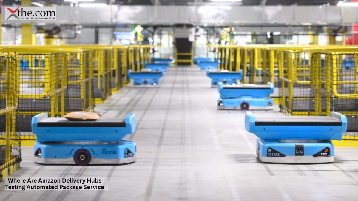
When a regional freight truck arrives at one of these neighborhood nodes, it doesn’t unload into a warehouse with human sorters. Instead, packages go into an automated system with scanning tunnels, gates, and conveyor belts that read each label and send each package to the right spot in less than two seconds. For example, a package for East Pine Street is sent to a specific cell in a modular storage matrix. A package flagged for pickup at an Amazon delivery innovation high-density automated packaging center is directed to a dedicated output lane that feeds directly into a bank of automated lockers. 

These lockers are more advanced than the standard Amazon Hub units found in Whole Foods. The Seattle test lockers are climate-controlled, so items like groceries and temperature-sensitive medicines can be stored safely in special sections. Customers receive a one-time PIN via the Amazon app, then walk or drive to the nearest node most have a small drive-through area and pick up their package without assistance from staff. 

Removing manual sorting is a big deal. In traditional last-mile delivery, hands-on sorting at a station takes 18 to 22 minutes per package, according to supply chain analysts who reviewed Amazon’s efficiency reports. High-density supply nodes cut out almost all of that time. The automated system does in seconds what used to take minutes. 

The Risk Calculus Amazon Is Running 

Every pilot program comes with risks. Amazon’s Seattle tests have at least three main risks that company leaders are watching closely. 

The first risk is whether customers will use the lockers. Automated lockers are less convenient for people accustomed to doorstep delivery. According to Amazon’s own research, reported by The Wall Street Journal in 2024, only about 34% of customers in dense cities choose lockers when given the option. The company is testing incentives, such as small discounts or Prime credits, to encourage more people to use them. 

The second risk is finding enough commercial space. To cover Seattle, Amazon needs to secure long-term leases or buy property, but commercial real estate prices are still high in the Pacific Northwest. The company has reportedly teamed up with at least two property investment groups to get key locations, but details haven’t been shared. 

The third risk is the optics of labor displacement. Amazon’s delivery innovation of this magnitude does not arrive without political scrutiny. Seattle’s city council has been among the most aggressive in the country in pushing for gig worker protections and delivery driver oversight. A network of facilities intended to decrease human handling of packages will face that legislative environment directly. 

The Wider Deployment Horizon 

Seattle isn’t the final stop. It’s the city where Amazon is proving its concept. The company has filed building permits in at least six other cities, including Chicago, Boston, and Austin. This shows Amazon sees its high-density automated packaging center model as something it can expand, not just test. Based on permits and investment reports, the main rollout is expected in 2026 and 2027. 

Competition is speeding up this timeline. Walmart’s GoLocal delivery network and FedEx’s SureDrop locker program are both growing in cities. While neither has matched Amazon’s combination of high-density supply nodes, last-mile drivers, and automated lockers, they are catching up. 

What This Signals for Urban Logistics 

The Seattle pilot is not only about Amazon. It shows where urban logistics is going as a whole. Cities are deliberately making it harder for traditional delivery systems. Changes in zoning, congestion pricing, and emissions rules in major U.S. cities are prompting delivery companies to adopt smaller, smarter, and more automated facilities. 

Amazon’s neighborhood-scale delivery innovation is a bet that the company best suited to lead urban logistics will be the one whose infrastructure blends in. This means being set up in commercial areas, automating the inventory handoff, and allowing customers to access packages when drivers aren’t available. 

We’ll soon see if Seattle’s early results support expanding this approach nationwide. The permits are already in place.

Source: Amazon News 

San Jose, California 

A single misread shadow of 70 miles per hour can cause serious problems. This is the challenge facing every autonomous vehicle program from Detroit to Shenzhen, and it is exactly what Sony’s new photonic sensing hardware aims to solve. 

Sony Sensor Evolution made a noticeable entrance. In the past three years, Sony’s semiconductor division has shifted from consumer imaging to automotive-grade LiDAR components, creating sensing blocks so well optimized that engineers in Silicon Valley are rethinking their hardware choices. The company’s SPAD (Single-Photon Avalanche Diode)- based detector arrays, now moving toward production, measure photon return times with nanosecond resolution. This allows for distance calculations accurate to within a few centimeters, even in direct sunlight. 

How Sony Sensor Evolution Is Rewriting Automotive Perception 

Sony made a clear engineering choice. Instead of building a full LiDAR system and competing with companies like Luminar or Ouster, Sony focused on the chip itself. This matters because the sensor IC is where latency starts or ends. 

Sony’s latest sensing ICs include what the company calls Spatial Telemetry Arrays, placed directly on the chip next to the photon-detection elements. In traditional designs, raw photodetector signals are sent off-chip to a separate DSP for time-of-flight calculations. Sony combines these steps. The Spatial Telemetry Arrays handle time-stamp binning, noise rejection, and depth-map generation inside the same silicon package that receives the infrared photons. This reduces per-frame processing latency by about 40 percent compared to two-chip designs, according to Sony’s presentation at the 2024 International Solid-State Circuits Conference. 

This latency difference is important in practical driving. At highway speeds, 40 milliseconds corresponds to about 2.5 feet of road that the system has not yet mapped. For a car changing lanes in heavy city traffic, 2.5 feet can be the difference between a safe move and a possible collision. 

The Role of Autonomous Navigation Chips in the Signal Chain 

Sony’s sensing ICs work together with other chips. They send processed depth data directly to Autonomous Navigation Chips, which handle path planning, obstacle detection, and real-time steering. The quality of data transfer between these chips affects how well the ADAS system performs in tough conditions like rain, low-light conditions, or reflective lane markings that can confuse standard detectors. 

Sony’s design stands out because the Autonomous Navigation Chips receive pre-classified spatial events instead of raw point clouds. Rather than sending 1.2 million raw XYZ coordinates per second for the navigation processor to interpret, Sony’s sensing IC labels the data as “static obstacle,” “moving object,” or “road surface” before it leaves the chip. Engineers at major automotive suppliers say this shifts the work of understanding the data earlier in the process, closer to the hardware and away from software. 

This approach is important for large systems. A standard 128-channel LiDAR running at 20 Hz creates point clouds that would overwhelm most processors if left unfiltered. By pre-classifying the data, Sony reduces the data volume by about 60 percent before it reaches the navigation layer. This lets the Autonomous Navigation Chips spend more time on decision-making instead of sorting through raw data. 

Sony Spatial Telemetry Arrays Autonomous Vehicle Sensor Integration: The Deployment Timeline 

Right now, every program manager at an OEM wants to know when this technology will show up in a real production vehicle, not just in a lab. 

Sony’s spatial telemetry arrays autonomous vehicle sensor integration is currently at the validation stage with at least two unnamed Tier 1 suppliers in Japan and Germany, according to Sony’s filings with Japan’s Financial Services Agency in early 2025. Mass production, defined as shipping at least 100,000 units per year with AEC-Q100 qualification, is planned for late 2026. This corresponds to the launch schedules for several next-generation ADAS platforms set for the 2027 model year. 

Sony’s engineering center in San Jose, which opened in 2023, plays a key role in this project. The facility has automotive-grade test chambers that can cycle chips through the full SAE temperature range, from -40 °C to 125°C, while running live LiDAR simulations. This is where Sony Sensor Evolution turns plans into concrete results. 

What Still Has to Happen Before Roads Get Smarter 

Getting hardware certified for automotive use is a serious process. Sony’s sensing ICs must pass the ISO 26262 ASIL-D functional safety certification, the highest level required for systems where failure could cause loss of life. This process usually takes 18 to 24 months for a new semiconductor design. Sony is doing this at the same time as supplier validation, taking on some risk to speed up the path to market. 

System-level calibration is another challenge. The Spatial Telemetry Arrays in the sensing IC are carefully calibrated at the chip level, but each vehicle has its own optical setup, including windshield shape, mounting vibrations, and temperature changes from the dashboard. Calibration activities that align chip specs with real-world vehicle conditions add more engineering work for OEM integration teams. 

None of these problems is impossible to solve. The semiconductor industry has handled even tougher integration problems. However, this means there is no single date for when the technology will be ready. Instead, it is a process: first, chip validation; then, system validation; followed by regulatory approval; and finally, mass production. 

The Competitive Pressure Shaping Sony’s Pace 

Sony is entering a challenging automotive sensing market. Infineon, STMicroelectronics, and Onsemi are all active at the photodetector level. What sets Sony apart is a decade of SPAD research from its consumer camera division, originally developed for low-light smartphone photography, now used in a market with much higher profit margins than consumer electronics. 

The automotive LiDAR component market is expected to reach $6.8 billion per year by 2030, according to Yole Group’s 2024 market analysis. Sony’s chip design reduces the computational load and improves depth precision, giving the company a structural advantage rather than just a small technical improvement. 

Roads are set to become smarter. The real question was never about whether autonomous systems could map the world accurately enough. Thanks to Sony’s work on sensing technology, the question now is how soon the supply chain can deliver this hardware at scale. That answer is closer now than it was two years ago.

Source: Company News & Media Relations 

Santa Clara, California 

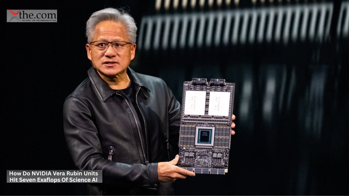
Seven exaflops means seven million trillion floating-point operations per second. This is not simply a marketing claim; it is the actual measured output of a single NVIDIA Vera Rubin platform rack. Just three years ago, this level of computing power would have seemed impossible even in a national supercomputing center. The organizations using this architecture are not focused on breaking records. Their goal is to shorten the time from a scientific hypothesis to a verified result, from months to minutes. 

The Architecture Behind the Number 

The NVIDIA Vera Rubin platform combines two types of chips in one server rack: the Rubin GPU, which uses advanced memory with stacked HBM4 pools, and the Vera CPU, NVIDIA’s first in-house general-purpose processor based on its Grace line but redesigned for science. Instead of using a standard PCIe bus, these chips connect through fifth-generation NVLink channels, which provide over 1.8 terabytes per second of two-way bandwidth between every GPU and CPU in the rack. 

That bandwidth is important. In agentic scientific computing, where self-directed software agents read sensor data, run simulations, verify results, and adjust resources without waiting for humans, the delay between the CPU’s control and the GPU’s calculations is the primary bottleneck. NVLink removes the bottleneck that used to slow down these agents by forcing them to wait for slower connections. 

For example, imagine an aerodynamics model simulating turbulent airflow over a hypersonic vehicle. This simulation creates terabytes of data every second. In a typical setup, this data moves from GPU memory across PCIe, into DRAM, through a network switch, and back, adding small delays at each step. With the Vera Rubin rack, the agent running the simulation reads data directly from GPU memory via NVLink, identifies unstable regions, and instantly adjusts the mesh resolution, all on the same hardware. This means the system not only computes faster but also corrects itself before errors spread. 

Native FP64 and Why It Changes the Calculus for Science 

Consumer graphics processing unit architectures have historically treated double-precision arithmetic as a second-class citizen, throttling native FP64 supercomputing performance to push single-precision throughput numbers for machine training benchmarks. The Rubin GPU reverses that priority for scientific workloads by sustaining full-rate FP64 throughput without clock or core penalties. 

This is especially important for climate simulation. A global atmospheric model with 1-kilometer resolution, detailed enough to resolve individual storm cells, requires FP64 calculations to remain accurate over decades of simulation. If precision drops, errors accumulate, and the results become unrealistic. Because the NVIDIA Vera Rubin platform supports native FP64 supercomputing, climate centers like the European Center for Medium-Range Weather Forecasts can run these detailed models and their neural network post-processing on the same hardware. This removes the requirement for separate CPU-based supercomputers for high-accuracy physics. 

The NVIDIA Vera Rubin platform supercomputers for science agentic AI extend this exactness capability into a feedback loop. An agent overseeing a 50-year climate projection can detect when ensemble members are diverging beyond physically plausible bounds, halt those branches, and reallocate their compute budget to better-constrained initial conditions—all in FP64, all without a human operator in the loop. 

Where the Units Are Going: A Global Deployment Picture 

National laboratories are the first to use these systems. Argonne National Laboratory near Chicago is adding Vera Rubin racks to speed up its Aurora successor project. Lawrence Berkeley National Energy Research Scientific Computing Center has chosen Vera Rubin as its main GPU for the next round of projects. In Europe, the Jülich Supercomputing Center in Germany and CINECA in Italy are adding these units to their pre-exascale systems, which support the EuroHPC Joint Undertaking’s research groups. 

The Japanese National Institute for Fusion Science uses agentic scientific computing on Vera Rubin hardware to control plasma in real time during tokamak experiments. In this case, the agent processes data from hundreds of sensors and adjusts magnetic coils within microseconds. This is not a batch job but a perpetual, closed-loop process that needs the fast CPU-GPU connection provided by NVLink in the Vera Rubin rack. 

The Agentic Layer: Software That Thinks About Science 

Hardware alone is not enough for agentic scientific computing. The software built on the NVIDIA Vera Rubin platform, especially NVIDIA’s NIM microservices and OpenAI’s open standards, lets researchers set scientific goals directly rather than writing step-by-step instructions. For example, a researcher can ask whether there is a statistically significant link between ocean temperature changes and jet stream shifts over 40 years. The agent then breaks this down into smaller tasks, assigns GPU resources, runs tests, and returns ranked results along with uncertainty estimates. 

This is what the NVIDIA Vera Rubin platform supercomputers for science agentic AI: it does not replace scientists but gives them computing tools that let scientific questions be answered as fast as the hardware allows, instead of being limited by human workflow speed. 

The Seven-Exaflop Threshold as a Scientific Inflection Point 

When you have seven exaflops per rack and multiply that by 50 or 100 racks in a facility, you get so much computing power that it changes what kinds of questions scientists can ask. Protein folding simulations that once needed special campaigns on national supercomputers can now run in the background. Seismic hazard models for entire tectonic plates, in great detail, can become regular quarterly updates rather than huge, rare projects. 

The bigger change is at the institutional level. Facilities using the NVIDIA Vera Rubin platform are not just faster than older systems. They create an environment where agentic scientific computing and native FP64 supercomputing converge to form a new kind of research infrastructure one that actively participates in the scientific process, not just supports it. Scientists who adapt their procedures to these systems in the next few years will have a growing advantage in the decade ahead. 

Source: NVIDIA Vera Rubin Delivers World-Class Supercomputers for Science 

Austin, Texas  

At 2:47 a.m. on a Tuesday, a flood of HTTP requests hit the servers of a mid-sized financial data publisher. The requests looked almost human, arriving at staggered intervals, using rotating user agents, and copying browser fingerprints from real Chrome sessions in São Paulo and Stockholm. But they were not quite real. Within 11 seconds, Cloudflare Bot Management flagged the entire cluster, isolated the traffic, and quietly blocked it. There was no CAPTCHA and no redirect. The attack simply disappeared. The publisher never knew it happened, and that invisibility is intentional. 

How Cloudflare Bot Management Became the Quiet Enforcer of the Web 

The web scraping industry has grown quickly. What started as a small group using basic Python scripts to collect data has turned into a complex shadow economy. Now, machine learning models power these tools, copying real user behavior with surprising accuracy. The people behind them are not just curious teenagers. They are organizations building private datasets to train large language models, and they want your content. 

Cloudflare’s response to this evolution is not a single product feature. It is an architectural concept. The company’s behavioral analysis firewall module an element of its broader Cloudflare bot management generative scraper defense update released in recent months monitors not just what a request looks like, but how it moves. Timing between clicks. Mouse entropy. The sequence in which JavaScript objects are evaluated. These signals, aggregated across Cloudflare’s network of over 20 million internet properties, allow the system to build a behavioral fingerprint that a spoofed user agent just cannot replicate. 

The New Face of Automated Indexing: Why Traditional Defenses Fall Short 

For years, rate limiting was the standard solution. If something hits an endpoint more than 60 times per minute, and you have covered most of your exposure. That logic no longer works. Today’s generative scraper defenses must contend with bots that deliberately throttle themselves operating at 3 to 4 requests per minute, perfectly within normal human browsing thresholds, but running 40,000 concurrent sessions across a botnet of residential proxies. 

The range of targets has also grown. AI-powered scrapers do not just go after public web pages. They look for data on API endpoints, chain authenticated sessions, and exploit JavaScript-rendered content that older firewalls struggle to handle. When a scraper can solve a CAPTCHA using a third-party service for less than $2 per 1,000 attempts, the cost of detection becomes almost nothing. 

This situation led Cloudflare to rebuild its detection system from the ground up. The latest module collects data from the TLS handshake before any HTML is sent. It looks at browser cipher suite order, JA3 fingerprint differences, and HTTP/2 frame patterns. All of this information goes into a scoring model that rates each session’s chance of being a bot in real time. Publishers using this system have caught scraper clusters that were secretly collecting content for weeks. 

AI Traffic Safeguards: The Policy Layer That Machines Cannot Social-Engineer 

Detection by itself is not enough. Once a session is flagged, the next question is what to do about it. Cloudflare’s solution uses a tiered response system that avoids simply blocking traffic. Instead, it adds carefully chosen obstacles, a strategy with clear reasoning behind it. 

Hard blocks help scrapers learn. If a bot receives a 403 error immediately after triggering a detection rule, the operator knows the cause and can adjust tactics. Instead, Cloudflare’s AI traffic safeguards use what the industry calls “tarpit” responses. These connections accept the bot’s session, respond slowly, and send back either empty or degraded data. The scraper wastes resources and gets nothing useful. The operator does not change anything, because everything seems normal from their side. 

This has significant consequences for organizations that train generative AI models on scraped data. A model trained on poisoned or degraded web content does not fail in obvious ways. Instead, it fails quietly, with subtle biases that might not surface until months later. Some content owners are now exploring whether feeding scrapers strategic misinformation is a legally ambiguous area or a valid defense. 

The Stakes for Publishers, Enterprises, and the Wider Information Economy 

Cloudflare has reported that AI-related crawler traffic rose by over 50% in 2024. Much of this traffic comes from undisclosed operators bots that do not identify themselves in the user agent and ignore robots.txt rules. The most targeted content includes legal databases, medical literature, financial filings, and news archives. 

For a regional newspaper, this traffic results in higher server costs with no extra revenue. For a pharmaceutical research firm, it could mean their clinical summary data ends up in a competitor’s training set. The main idea behind Cloudflare bot management is property rights: your content belongs to you, and its protection should correspond to its value. 

The latest behavioral analysis modules show that the industry agrees passive defenses like robots.txt, IP blocklists, and rate limiting are not enough against attackers who keep improving their tools. Now, the system needs active intelligence tools that learn the behavior of new scrapers as soon as they appear, not weeks later after the damage is done. 

The Asymmetry That Defines the Next Chapter 

Scraper operators have one big advantage: they only need to find one way through the defenses. Defenders, on the other hand, must block every possible path. Generative scraper defenses try to fix this unevenness by making it so costly to evade detection that stealing content is no longer worth it. 

Whether Cloudflare’s behavioral layer can keep up depends on how fast attackers adapt. In the past, they have always advanced more quickly than defenders would like. The 2:47 a.m. block in Austin protected one publisher for one night. But as this system is used across 20 million properties, it starts to act like an immune system, making it harder for ghost scrapers to go unnoticed.

Source: The Cloudflare Blog 

Redmond, Washington  

Picture an IT administrator arriving Monday morning to find that hundreds of workstations across a corporate campus have stopped loading Windows entirely. No blue screen, no error message, just a black void at startup. That scenario, once theoretical, edges closer to reality every month that organizations running legacy hardware ignore the quiet countdown on their Microsoft Secure Boot certificate expiration. 

The 15-Year Clock No One Watched 

When Microsoft and firmware vendors embedded the first Secure Boot signing certificates in UEFI chips in 2011, they set a firm 15-year expiration. This is not a flexible deadline or one rolling window, but a strict cryptographic limit. These certificates will expire in mid-2026, and any machine that checks signatures against the old root will no longer trust a bootloader after that date. 

The Microsoft Secure Boot certificate expiration is not a patch Tuesday footnote. It affects every PC manufactured roughly between 2012 and 2016 that has not received a firmware update layering in the 2023 replacement certificate block. Gartner estimated in 2024 that roughly 240 million PCs worldwide remain on hardware more than five years old. A non-trivial slice of those machines carries the 2011-era certificate chain and nothing newer. 

How Secure Boot Actually Works — And Why Certificates Matter 

Secure Boot is a UEFI standard that stops unauthorized code from running during the pre-OS boot process. Before Windows gives control to the kernel, the firmware checks each component’s digital signature against a database of trusted keys stored in UEFI non-volatile memory. The KEK trust anchors, or Key Exchange Keys, are positioned one layer below the Platform Key and one layer above the database of allowed signatures. They serve as gatekeepers, authorizing updates to what the system recognizes as legitimate boot software. 

When the certificate used to sign a bootloader expires, firmware that strictly checks timestamps will reject that signature. The machine will not boot. This is not a bug; it is how the security model is supposed to work. The issue is that most organizations have never had to consider KEK trust anchors expiring before, since this is the first time Secure Boot certificates are reaching the end of their lifespans. 

The Microsoft Secure Boot certificate expiration June 2026 UEFI update addresses precisely this gap by including the 2023 Windows UEFI CA certificate and updated Secure Boot Forbidden Signature Database entries, packaged in a way that Windows Update, SCCM, and Intune can send to enrolled devices. This update adds the new certificate to the UEFI DB and KEK stores, so the firmware will continue to recognize Microsoft-signed bootloaders as trusted after the old certificate expires. 

UEFI Security Updates: The Deployment Problem at Scale 

Rolling out UEFI security updates across several types of devices is much more complex than installing a browser patch. Writing to UEFI non-volatile memory needs higher-level firmware access, and on some hardware, the update only works properly if the system follows a specific restart process. If the update is performed incorrectly, it can corrupt the Secure Boot database, leaving the machine unable to trust either the old or the new certificate. 

Microsoft’s recommended fix uses a multi-step script. PowerShell modules first check the current KEK and DB contents, then prepare the new certificate, and finally trigger a firmware update during the next clean restart. For administrators using Windows 11 22H2 or later, this process usually happens automatically through Windows Update, as long as the device is managed, and the update is not blocked by a compatibility hold. 

The bigger challenge is with Windows 10 machines nearing end-of-support in October 2025, as well as devices that run third-party Linux distributions alongside Microsoft’s Secure Boot. These systems require manual updates and custom scripts to add the 2023 certificate to the appropriate UEFI stores. If this step is skipped on firmware that strictly enforces the rules, the machine will not be able to boot any Microsoft-signed shim or bootloader after June 2026. 

Firmware Rollovers and the Risk of Getting Them Wrong 

In the industry, replacing one set of trust material with another is called a firmware rollover, and it is one of the most sensitive tasks in enterprise IT. Unlike software updates, which can usually be rolled back if something goes wrong, a failed firmware rollover can render a device unbootable, with no way to fix it via software. In these cases, you may need physical access to reset UEFI settings or, in the worst situations, replace the motherboard. 

This is why Microsoft’s recommended scripted deployment includes a validation step before making any permanent changes. The script reads the new certificate from UEFI memory and checks its hash against the expected value. Only if the comparison matches does the process mark the device as fixed. If there is a mismatch, the script tries to roll back the change and flags the device for manual review. 

Organizations using Microsoft Configuration Manager can track remediation status through compliance baselines tied to the presence of the 2023 certificate thumbprint in the firmware store. Those running Intune have access to pre-built compliance policies that query the same data through the device health attestation service. 

What Happens if Organizations Miss the Window 

A machine that has not been updated will not always stop working right at midnight when the certificate expires. How the firmware behaves depends on whether it checks timestamps strictly or allows more flexibility. Many consumer UEFI systems are more permissive, whereas enterprise firmware from Dell, HP, and Lenovo usually adheres more closely to the rules. 

The risk increases during recovery situations. A machine that works fine now might not recover from a BitLocker lockout, a failed update, or a boot sector repair. In these cases, the recovery environment checks signatures again from the beginning. At that point, an expired certificate becomes a serious problem, not just a compliance issue. 

The most proactive organizations are not waiting to find out which of their machines strictly enforce the standard. They are already running inventory scripts, finding devices that only have the 2011 certificate, and planning firmware rollovers during their regular change management periods before summer. 

The Microsoft Secure Boot certificate expiration is an infrastructure deadline that benefits organizations that treat it as a planned migration rather than an emergency. The certificate expires on a set date, and the chance to handle it smoothly will not last forever.

Source: Introducing the next Surface Pro and Surface Laptop, built for performance and flexibility 

Austin, Texas 

Every so often, a new technical education program comes along that changes who gets to shape the future. AMD’s choice to launch its free global Microchip Design Academy in Austin, Texas, is one of those moments. The AMD Tech Training program isn’t merely a corporate goodwill project. It is a tactical move that lets AMD help train the next generation of chip architects, software engineers, and hardware innovators before other companies even notice the talent pipeline is forming. 

Why Austin, and Why Now for AMD Tech Training 

Austin was not chosen by chance. The city now has more semiconductor-related engineering talent per person than almost any city outside Silicon Valley. With Samsung’s Taylor factory, Tesla’s engineering headquarters, and the University of Texas producing thousands of electrical engineers each year, AMD saw a strong opportunity. The AMD Tech Training academy connects directly to this ecosystem, providing global learners with free access to basic chip design education, with Austin as the main hub. 

The timing matters too. Washington’s CHIPS Act has poured over $52 billion into domestic semiconductor manufacturing, creating an acute skills shortage. Industry analysts at the Semiconductor Industry Association estimated in 2024 that the U.S. alone will face a deficit of approximately 67,000 chip engineers by 2030. AMD is not waiting for universities to close that gap. 

Open Silicon Architecture: The Curriculum’s Technical Core 

What makes this academy different from a typical coding bootcamp or online certificate program is its focus on hardware instruction. The curriculum is built around Open Silicon Architecture, which is an open chip design model that lets developers’ study, modify, and test processor blueprints without paying for special licenses. 

AMD has shared open-source silicon simulation blueprints along with its live hardware developer workshops. Students work with real instruction-set documents, register-transfer-level design files, and pre-synthesis netlists. This is not just the theory from slides. It is hands-on experience with the same basic schematics that AMD’s own teams use when testing new processor architectures. 

The Open Silicon Architecture curriculum also includes RISC-V toolchains, providing participants with a framework they can use wherever they work in the future. Graduates of this program will understand not only AMD’s ecosystem but also the wider open hardware design language that is becoming standard in the industry. 

Developer Toolkits: From Simulation to Silicon 

Design education needs the right tools to be effective. The academy’s Developer Toolkits may be its most practical feature. Participants get access to a selected set of EDA (Electronic Design Automation) software, simulation environments, and FPGA emulation boards. These are the same types of tools that usually cost companies tens of thousands of dollars each year. 

The Developer Toolkits are organized into three levels. Beginners start with software simulations, writing HDL (Hardware Description Language) code, and checking logic with automated testbenches. Intermediate learners use FPGA-based prototyping, running their designs on hardware that acts like future silicon. Advanced groups gain access to AMD’s specialized pre-silicon verification environments, which are typically available only to full-time engineers. 

This step-by-step approach is intentional. AMD is building a talent pipeline that turns beginners into job-ready specialists in 18 to 24 months. 

The AMD Open Silicon Architecture Developer Tech Training Program’s Global Reach 

The academy’s biggest goal is its international reach. Austin is the main headquarters, but the AMD Open Silicon Architecture Developer Tech Training Program also runs online groups and plans regional workshops in Europe, Southeast Asia, and sub-Saharan Africa. The clear aim is to give independent developers everywhere direct access to basic instruction, no matter how close they are to major semiconductor centers. 

Think about a developer in Nairobi or Bucharest who cannot afford traditional chip design training. Usually, the only options are costly graduate degrees or entry-level jobs at companies that may not be available locally. The AMD open silicon architecture developer tech training program changes this. Now, anyone with a laptop and a good internet connection can follow the same curriculum as someone attending in Austin. 

The focus on instant software improvement is especially important. As AMD prepares to launch its next-generation personal processors, which will follow the Ryzen and EPYC lines, the company needs developers worldwide who already know how to write software that delivers peak performance from these chips as soon as they are released. In the past, this kind of optimization happened after launch, as outside developers learned the hardware over time. AMD is speeding up that process by training developers before the chips are even available. 

What This Means for the Competitive Landscape 

Intel has the oneAPI initiative. Qualcomm works with academic partners. NVIDIA’s CUDA ecosystem has built developer loyalty for almost twenty years. AMD’s academy is not a copy of these programs. Instead, it takes a different approach by combining open-source credibility, structured professional development, and a clear focus on software engineers who understand hardware. 

This difference is important because the upcoming major advance in computing will not come from faster clock speeds alone. It will come from developers who know how to write code that fully leverages chip-level parallelism, cache systems, and memory throughput—skills that most software engineers lack. AMD believes that if it trains enough of these developers, using its own architecture as the main example, the business benefits will follow. 

A Deliberate Bet on Open Infrastructure 

By focusing its academy on Open Silicon Architecture and easy-to-access Developer Toolkits, AMD is making its long-term intentions clear. Closed, proprietary systems may keep developers for a while, but they often lead to frustration over time. Open frameworks help build communities, and those communities create tools, documentation, and support that no marketing budget can match. 

The Austin academy, along with its global online reach through the AMD open silicon architecture developer tech training program, is far more than a corporate training effort. It is a decision about who AMD wants to build on its platforms over the next twenty years, and the answer is simple: anyone who wants to learn.

Source: AMD Community Updates 

Cupertino, California  

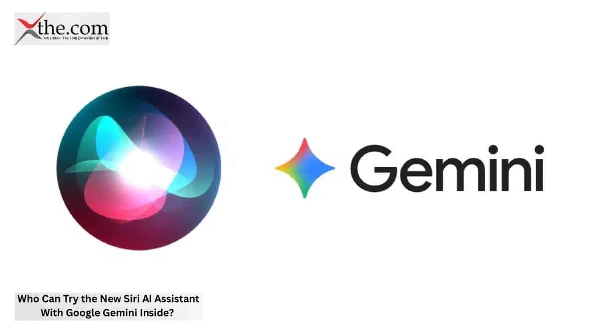
The waitlist just got shorter. As of this week, Apple has opened a dedicated developer channel for testing its most substantive re-engineering of Siri since the assistant launched in 2011. The stakes are high: Apple introduces Siri AI not as a cosmetic upgrade but as a ground-up architectural overhaul, one that routes complex queries through Google’s Gemini infrastructure while keeping sensitive personal data anchored locally on-device. Developers enrolled in the Apple Developer Program can begin API testing today, and what they find will likely determine whether this gamble pays off. 

How Apple Introduces Siri AI With a Fundamentally New Architecture 

The key change in the new Siri is behind the scenes. Siri’s intelligence now works in two layers. The first is a small model that runs only on your device. It handles things like calendar entries, messages, and what’s on your screen, all without sending data to external servers. The second layer sends more complex tasks, such as research or drafting long documents, to Gemini’s cloud via Apple’s Private Cloud Compute system. 

This setup is called the Apple Intelligence Architecture. It decides where each query should go. For example, if you ask Siri to find an email from a supplier and write a reply that summarizes earlier conversations, the on-device model reads your screen and gathers context. Gemini then handles the more complex writing. You get one smooth response, and you won’t notice the switch between models. 

Onscreen Awareness: The Feature That Changes Developer Calculus 

One of the biggest new features in Apple’s technical documentation is Onscreen Awareness. Siri can now understand whatever is on your screen, like a PDF contract, a live spreadsheet, or a webpage. It uses this visual context in its responses, so you don’t have to copy, paste, or describe what you see. 

Here’s an example: a procurement executive looks at a supplier quote in Safari and asks Siri, “Does this pricing match what we agreed on in March?” Siri reads the document on the screen, checks the March email conversation stored on the device, and points out any differences. The user doesn’t have to leave the screen or switch apps. This is a big change from the old, keyword-based Siri. 

For developers, Onscreen Awareness creates new API possibilities. Companies making internal tools can now let Siri respond to what’s happening in real time, not just to fixed commands. For example, a field technician’s app could let Siri read a schematic on the screen and answer questions right away. Apple’s developer documentation includes three examples of this kind of live-context integration. 

Gemini Integration: What It Means to Outsource Reasoning 

The Gemini Integration in the new Siri should be looked at carefully, not just celebrated or criticized. Only queries that the on-device model can’t handle are sent to Gemini, and only if the user has chosen to use these extra AI features during setup. Apple’s privacy white paper says that Gemini does not receive any persistent user identifiers, and neither Apple nor Google retains query data for training their models. 

Still, legal and compliance teams at companies should review the details before enabling Siri’s extra features on work devices. Queries sent to the Gemini integration pass through Apple’s Private Cloud Compute nodes, which Apple says are temporary and can be audited. However, outside experts have not yet confirmed these claims, and security researchers such as Trail of Bits have raised concerns. 

For most regular users, this setup is simple. If you ask Siri to explain a complex research paper or create a detailed travel plan, Gemini handles the big-picture reasoning for you. You don’t have to do anything special—Apple manages everything in the background. 

Who Gets Access Now? 

Right now, developers in the United States, the United Kingdom, Canada, Australia, and New Zealand can access the new Siri API through the Apple Developer Program. Apple says more regions, including the European Union, will get access later, but there’s no set timeline yet. Users with iOS 19 or macOS Sequoia or newer on supported devices like the iPhone 16 series and M-series Macs can enable the new Siri features in the Intelligence & Search settings. 

Enterprise customers using Apple Business Manager can choose which intelligence features employees can use. IT administrators have fine-grained control over whether only on-device features or full Gemini-assisted capabilities are enabled. 

Apple Introduces Siri AI Powered by Apple Intelligence and Gemini — What Developers Should Test First 

Apple introduces Siri AI powered by Apple Intelligence, and Gemini brings three main API endpoints for developers to explore right away. These are: SiriKit Intent Definition for in-app Onscreen Awareness, the Natural Language Escalation API to decide which queries go to Gemini, and the Context Window Extension, which lets third-party apps send background data into a Siri session. 

Developers who act fast will get a real advantage. The first business apps built on Apple Intelligence Architecture, using both local context and Gemini’s advanced features, will probably set the standard for productivity software on Apple devices for years to come. The architecture is ready, and the API documentation is available. Now it’s just a matter of who gets started first.

Source: Apple introduces Siri AI, a profoundly more capable and personal assistant